The following content is an automatically extracted verbatim text
from the original manufacturer datasheet and is provided for reference purposes only.
View original datasheet text
www.DataSheet4U.com
MOTOROLA
SEMICONDUCTOR TECHNICAL DATA
Order this document by VN2222LL/D
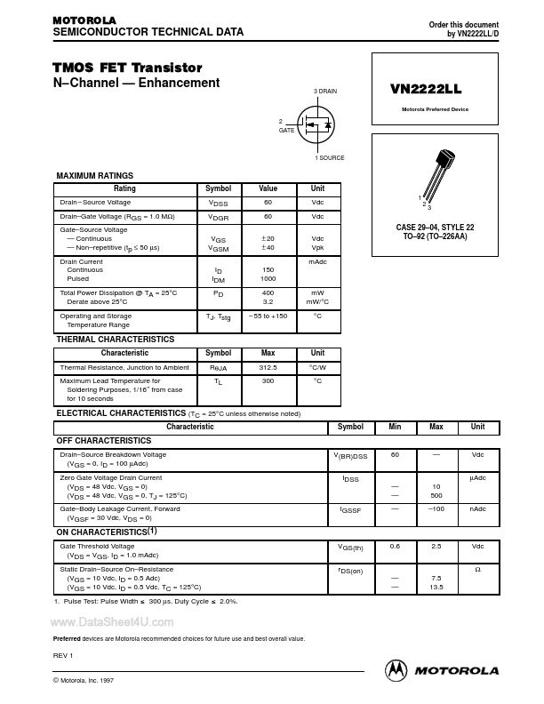
TMOS FET Transistor
N–Channel — Enhancement
2 GATE 3 DRAIN
VN2222LL
Motorola Preferred Device
1 SOURCE
MAXIMUM RATINGS
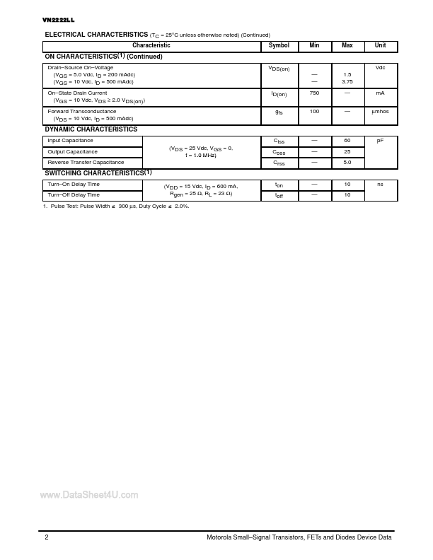
Rating Drain – Source Voltage Drain–Gate Voltage (RGS = 1.0 MΩ) Gate–Source Voltage — Continuous — Non–repetitive (tp ≤ 50 µs) Drain Current Continuous Pulsed Total Power Dissipation @ TA = 25°C Derate above 25°C Operating and Storage Temperature Range Symbol VDSS VDGR VGS VGSM ID IDM PD TJ, Tstg Value 60 60 ± 20 ± 40 150 1000 400 3.
 VN2222LL Datasheet