The following content is an automatically extracted verbatim text
from the original manufacturer datasheet and is provided for reference purposes only.
View original datasheet text
MOTOROLA
SEMICONDUCTOR TECHNICAL DATA
Order this document by MTD20P03HDL/D
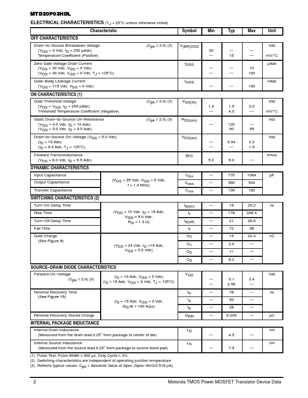
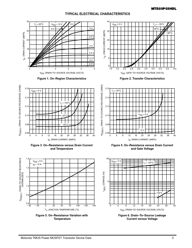
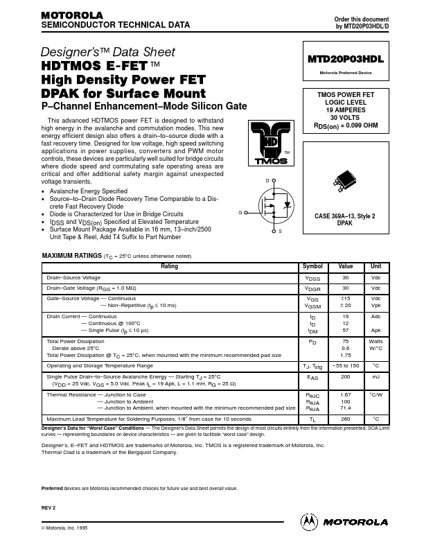
™ Data Sheet HDTMOS E-FET.™ High Density Power FET DPAK for Surface Mount
Designer's
MTD20P03HDL
Motorola Preferred Device
P–Channel Enhancement–Mode Silicon Gate
This advanced HDTMOS power FET is designed to withstand high energy in the avalanche and commutation modes. This new energy efficient design also offers a drain–to–source diode with a fast recovery time. Designed for low voltage, high speed switching applications in power supplies, converters and PWM motor controls, these devices are particularly well suited for bridge circuits where diode speed and commutating safe operating areas are critical and offer additional safety margin against unexpected voltage transients.
 MTD20P03HDL Datasheet