MC74AC534
MC74AC534 is OCTAL D-TYPE FLIP-FLOP manufactured by Motorola Semiconductor.
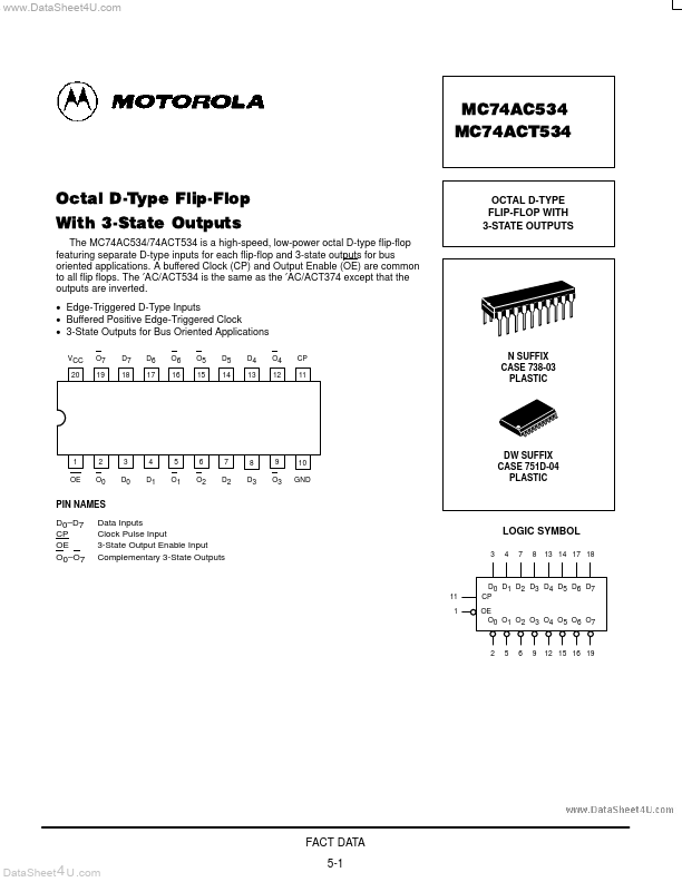
DESCRIPTION
The MC74AC534/74ACT534 consists of eight edge-triggered flip-flops with individual D-type inputs and 3-state true outputs. The buffered clock and buffered Output Enable are mon to all flip-flops. The eight flip-flops will store the state of their individual D inputs that meet the setup and hold times requirements on the LOW-to-HIGH Clock (CP) transition. With the Output Enable (OE) LOW, the contents of the eight flip-flops are available at the outputs. When the OE is HIGH, the outputs go to the high impedance state. Operation of the OE input does not affect the state of the flip-flops.
LOGIC DIAGRAM
D0 CP CP Q D CP D Q CP D Q CP D Q CP D Q CP D Q CP D Q CP D Q D1 D2 D3 D4 D5 D6 D7
OE O0 O1 O2 O3 O4 O5 O6 O7
Please note that this diagram is provided only for the understanding of logic operations and should not be used to estimate propagation delays.
MAXIMUM RATINGS-
Symbol VCC Vin Vout Iin Iout ICC Tstg Parameter DC Supply Voltage (Referenced to GND) DC Input Voltage (Referenced to GND) DC Output Voltage (Referenced to GND) DC Input Current, per Pin DC Output Sink/Source Current, per Pin DC VCC or GND Current per Output Pin Storage Temperature Value
- 0.5 to +7.0
- 0.5 to VCC +0.5
- 0.5 to VCC +0.5 ±20 ±50 ±50
- 65 to +150 Unit V V V m A m A m A °C
- Maximum Ratings are those values beyond which damage to the device may occur. Functional operation should be restricted to the Remended Operating Conditions.
REMENDED OPERATING CONDITIONS
Symbol VCC Vin, Vout Supply Voltage DC Input Voltage, Output Voltage (Ref. to GND) VCC @ 3.0 V tr, tf Input Rise and Fall Time (Note 1) ′AC Devices except Schmitt Inputs VCC @ 4.5 V VCC @ 5.5 V tr, tf TJ TA IOH IOL Input Rise and Fall Time (Note 2) ′ACT Devices except Schmitt Inputs Junction Temperature (PDIP) Operating Ambient Temperature Range Output Current
- High Output Current
- Low
- 40 25 VCC @ 4.5 V VCC @ 5.5 V...