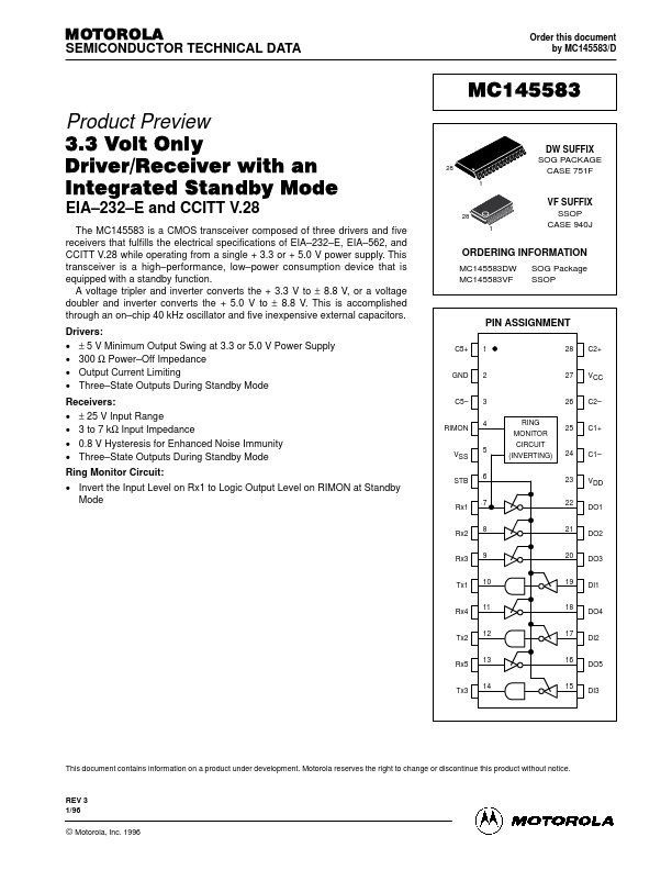
Datasheet4U Logo Datasheet4U.com

MC145583 - 3.3 Volt Only Driver/Receiver with an Integrated Standby Mode

General Description

VCC Digital Power Supply (Pin 27) This digital supply pin is connected to the logic power supply.

This pin should have a not less than 0.33 µF capacitor GND.

232 E connector (Pin 7) as we

Key Features

  • rter, which generate the VDD and VSS voltages. Rx1, Rx2, Rx3, Rx4, Rx5 Receive Data Inputs (Pins 7, 8, 9, 11, 13) These are the EIA.
  • 232.
  • E receive signal inputs. A voltage between + 3 and + 25 V is decoded as a space, and causes the corresponding DO pin to swing to GND (0 V). A voltage between.
  • 3 and.
  • 25 V is decoded as a mark, and causes the DO pin to swing up to VCC. DO1, DO2, DO3, DO4, DO5 Data Outputs (Pins 22, 21, 20, 18, 16) These are the receiver digital o.

📥 Download Datasheet

Full PDF Text Transcription for MC145583 (Reference)

Note: Below is a high-fidelity text extraction (approx. 800 characters) for MC145583. For precise diagrams, and layout, please refer to the original PDF.

MOTOROLA SEMICONDUCTOR TECHNICAL DATA Order this document by MC145583/D MC145583 Product Preview 3.3 Volt Only Driver/Receiver with an Integrated Standby Mode 28 1 DW SUF...

View more extracted text
Volt Only Driver/Receiver with an Integrated Standby Mode 28 1 DW SUFFIX SOG PACKAGE CASE 751F EIA–232–E and CCITT V.28 The MC145583 is a CMOS transceiver composed of three drivers and five receivers that fulfills the electrical specifications of EIA–232–E, EIA–562, and CCITT V.28 while operating from a single + 3.3 or + 5.0 V power supply. This transceiver is a high–performance, low–power consumption device that is equipped with a standby function. A voltage tripler and inverter converts the + 3.3 V to ± 8.8 V, or a voltage doubler and inverter converts the + 5.0 V to ± 8.8 V. This is accomplished through an on–chip 40 k