Datasheet Summary
..
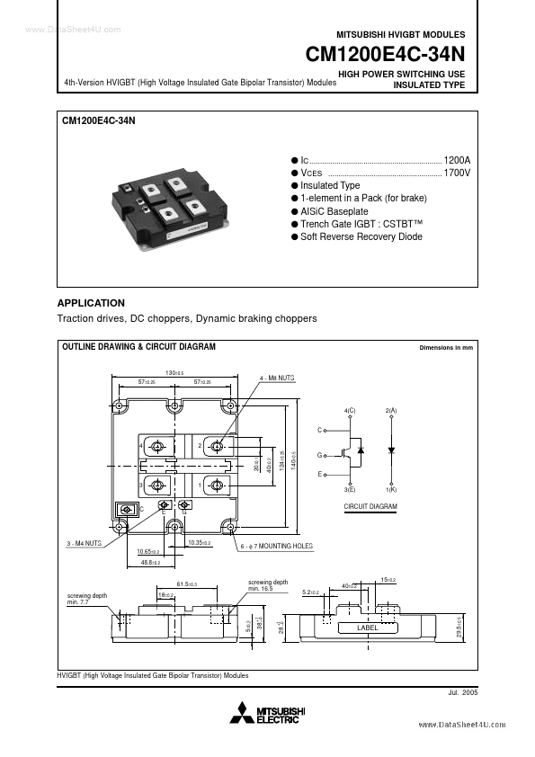
MITSUBISHI HVIGBT MODULES
4th-Version HVIGBT (High Voltage Insulated Gate Bipolar Transistor) Modules HIGH POWER SWITCHING USE INSULATED TYPE
CM1200E4C-34N q IC ................................................................ 1200A q VCES ....................................................... 1700V q Insulated Type q 1-element in a Pack (for brake) q AISiC Baseplate q Trench Gate IGBT : CSTBT™ q Soft Reverse Recovery Diode
APPLICATION Traction drives, DC choppers, Dynamic braking choppers
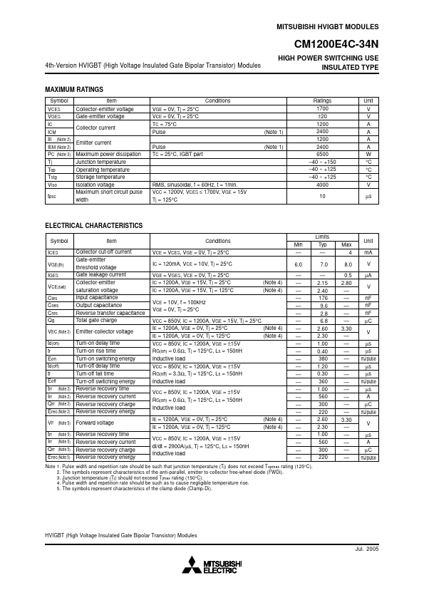
OUTLINE DRAWING & CIRCUIT DIAGRAM
130±0.5 57±0.25 57±0.25 4
- M8 NUTS
Dimensions in mm
4(C) C
2(A)
124±0.25 140±0.5 20±0.1 40±0.2
G E 3(E)...