CM100DC-24NFM
Description
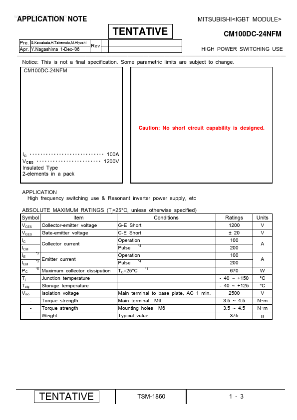
www.DataSheet4U.com APPLICATION NOTE MITSUBISHI<IGBT MODULE> TENTATIVE CM100DC-24NFM Pre. S.Kawabata,H.Takemoto,M.Hiyoshi Rev Apr. Y.Nagashima 1-Dec-'06 HIGH POWER SWITCHING USE ─────────────────...
www.DataSheet4U.com APPLICATION NOTE MITSUBISHI<IGBT MODULE> TENTATIVE CM100DC-24NFM Pre. S.Kawabata,H.Takemoto,M.Hiyoshi Rev Apr. Y.Nagashima 1-Dec-'06 HIGH POWER SWITCHING USE ─────────────────...