Datasheet4U Logo Datasheet4U.com

CGB7006-BD - MMIC or Packaged Matched Gain Block Amplifier

Download the CGB7006-BD datasheet PDF. This datasheet also covers the CGB7006-SC variant, as both devices belong to the same mmic or packaged matched gain block amplifier family and are provided as variant models within a single manufacturer datasheet.

Description

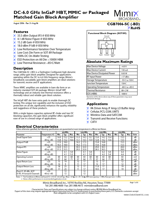
The CGB7006-SC (-BD) is a Darlington Configured, high dynamic range, utility gain block amplifier.

Designed for applications operating within the DC to 6.0 GHz frequency range, Mimix’s broadband, cascadable, gain block amplifiers are ideal solutions for transmit, receive and IF applications.

Features

  • 33.5 dBm Output IP3 @ 850 MHz 4.1 dB Noise Figure @ 850 MHz 15.2 dB Gain @ 850 MHz 18.0 dBm P1dB @ 850 MHz Low Performance Variation Over Temperature Low Cost: Die Form or SOT-89 Package 100% DC On-Wafer Testing ESD Protection on All Die: >1000V HBM Low Thermal Resistance:.

📥 Download Datasheet

Note: The manufacturer provides a single datasheet file (CGB7006-SC_MimixBroadband.pdf) that lists specifications for multiple related part numbers.

Datasheet Details

Part number CGB7006-BD
Manufacturer Mimix Broadband
File Size 601.55 KB
Description MMIC or Packaged Matched Gain Block Amplifier
Datasheet download datasheet CGB7006-BD Datasheet

Full PDF Text Transcription (Reference)

The following content is an automatically extracted verbatim text from the original manufacturer datasheet and is provided for reference purposes only.

View original datasheet text
DC-6.0 GHz InGaP HBT, MMIC or Packaged Matched Gain Block Amplifier August 2006 - Rev 31-Aug-06 CGB7006-SC (-BD) Functional Block Diagram (SOT -89) Ground 4 Features 33.5 dBm Output IP3 @ 850 MHz 4.1 dB Noise Figure @ 850 MHz 15.2 dB Gain @ 850 MHz 18.0 dBm P1dB @ 850 MHz Low Performance Variation Over Temperature Low Cost: Die Form or SOT-89 Package 100% DC On-Wafer Testing ESD Protection on All Die: >1000V HBM Low Thermal Resistance: <85ºC/Watt 1 Input 2 3 Ground Output Bias Absolute Maximum Ratings Max Device Voltage Max Device Current Max Device Dissipated Power RF Input Power Storage Temperature Junction Temperature Operating Temperature Thermal Resistance EDS (HBM) +6.0 V 130 mA 0.