SG3626
SG3626 is Dual High Speed Driver manufactured by Microsemi.
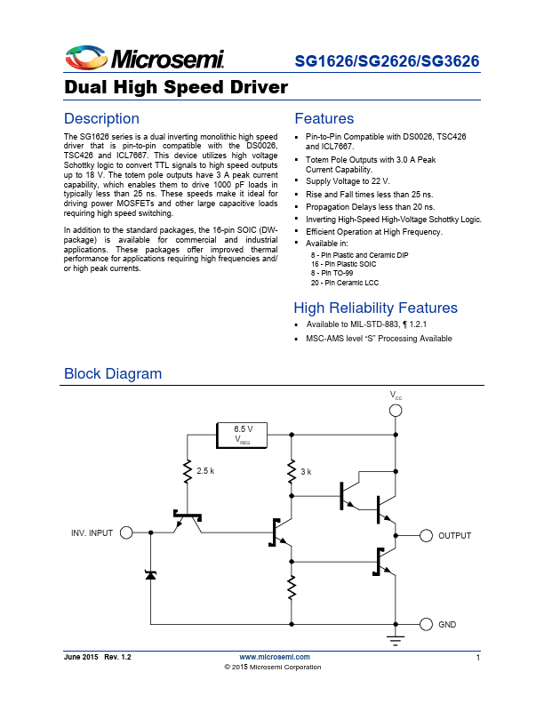
Description
The SG1626 series is a dual inverting monolithic high speed driver that is pin-to-pin patible with the DS0026, TSC426 and ICL7667. This device utilizes high voltage Schottky logic to convert TTL signals to high speed outputs up to 18 V. The totem pole outputs have 3 A peak current capability, which enables them to drive 1000 p F loads in typically less than 25 ns. These speeds make it ideal for driving power MOSFETs and other large capacitive loads requiring high speed switching.
In addition to the standard packages, the 16-pin SOIC (DWpackage) is available for mercial and industrial applications. These packages offer improved thermal performance for applications requiring high frequencies and/ or high peak currents.
Features
- Pin-to-Pin patible with DS0026, TSC426 and ICL7667.
- Totem Pole Outputs with 3.0 A Peak Current Capability.
- Supply Voltage to 22 V.
- Rise and Fall times less than 25 ns.
-...