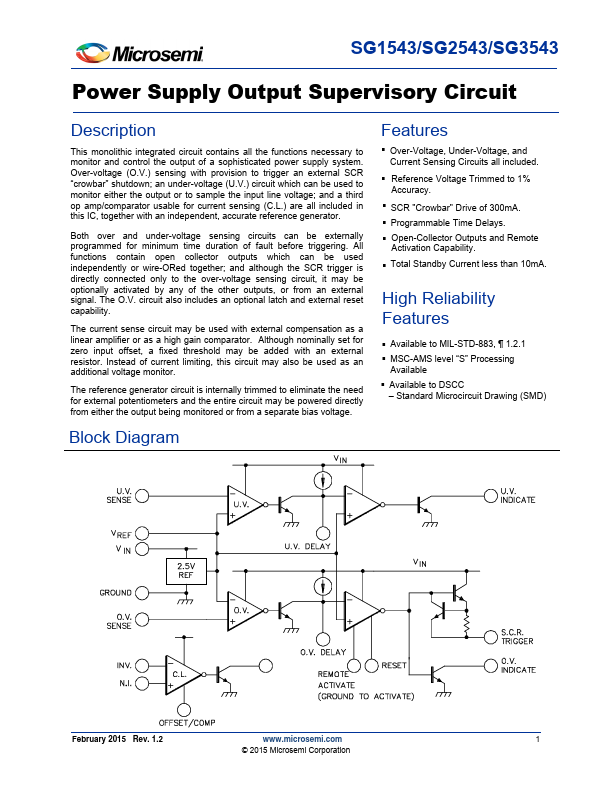
Absolute Maximum Ratings (Note 1)
Input Supply Voltage (+VIN)................................................. 40V
Sense Inputs ...................................................................... +VIN
SCR Trigger Current (Note 2) ......................................... 300mA
Indicator Output Voltage ..................................................... 40V
Note 1. Values beyond which damage may occur.
Note 2. At higher input voltages, a dissipation limiting resistor, RG
is required. See Figure 1.
Indicator Output Sink Current .......................................... 50mA
Operating Junction Temperature
Hermetic (J, L Packages) ............................................ 150°C
Plastic (N, DW Packages) ........................................... 150°C
Storage Temperature Range ............................ -65°C to 150°C
RoHS Peak package Solder Reflow Temp. (40 sec. max. exp.)..... 260°C (+0. -5)
Thermal Data
J Package:
Thermal Resistance-Junction to Case, θJC ............. 30°C/W
Thermal Resistance-Junction to Ambient, θJA .... .... 80°C/W
N Package:
Thermal Resistance-Junction to Case, θJC ............. 40°C/W
Thermal Resistance-Junction to Ambient, θJA ........ 65°C/W
DW Package:
Thermal Resistance-Junction to Case, θJC ............. 40°C/W
Thermal Resistance-Junction to Ambient, θJA ......... 95°C/W
L Package:
Thermal Resistance-Junction to Case, .................. 35°C/W
Thermal Resistance-Junction to Ambient, θJA ....... 120°C/W
Note A. Junction Temperature Calculation: TJ = TA + (PD x θJA).
Note B. The above numbers for θJC are maximums for the
limiting thermal resistance of the package in a standard
mounting configuration. The θJA numbers are meant to
be guidelines for the thermal performance of the
device/pc-board system. All of the above assume no
ambient airflow.
Recommended Operating Conditions (Note 3)
Input Supply Voltage (+VIN) .................................... 4.7V to 40V
Current Limit Common Mode
Input Voltage Range ........................................... 0V to +VIN -3V
Reference Load Current ........................................... 0 to 10mA
Indicator Output Voltage ......................................... 4.7V to 40V
Indicator Output Current ........................................... 0 to 10mA
Delay Timing Capcitor (Note 4) ........................... 0 to 1µF
Operating Ambient Temperature Range
SG1543 ....................................................... -55°C to 125°C
SG2543 ........................................................ -25°C to 85°C
SG3543 ........................................................ 0°C to 70°C
Note 3: Range over which the device is functional.
Note 4. Larger value capacitor may be used with peak current limiting. See Figure 7.
Electrical Characteristics
(Unless otherwise specified, these specifications apply over the operating ambient temperatures for SG1543 with -55°C ≤ TA ≤ 125°C, SG2543 with
-25°C ≤ TA ≤ 85°C, SG3543 with 0°C ≤ TA ≤ 70°C, and +VIN = 10V. Indicator outputs have 2kΩ pull-up resistor. Low duty cycle testing techniques
are used which maintains junction and case temperatures equal to the ambient temperature.)
Parameter
Supply Section
Input Voltage Range
Supply Current
Reference Section
Output Voltage
Line Regulation
Load Regulation
Short Circuit Current
Temperature Stability
Test Conditions
TJ = 25°C to TMAX
+VIN = 40V, Outputs open, TJ = 25°C
TJ = 25°C
+VIN = 5 to 30V
IREF = 0 to 10mA
VREF = 0V
SG1543/SG2543
Min. Typ. Max.
SG3543
Min. Typ. Max.
Units
4.5 40 4.5 40 V
4.7 40 4.7 40 V
7 10
7 10 mA
2.48 2.50 2.52 2.45 2.50 2.55 V
2.45 2.55 2.40 2.60 V
15
1 5 mV
1 10
1 10 mV
12 25 40 12 25 40 mA
.005 .005 %/°C
2