LX13049
TM ® VREF @ 800mV, 1.25A, 1.0MHZ PWM
PRODUCTION DATA SHEET
DESCRIPTION
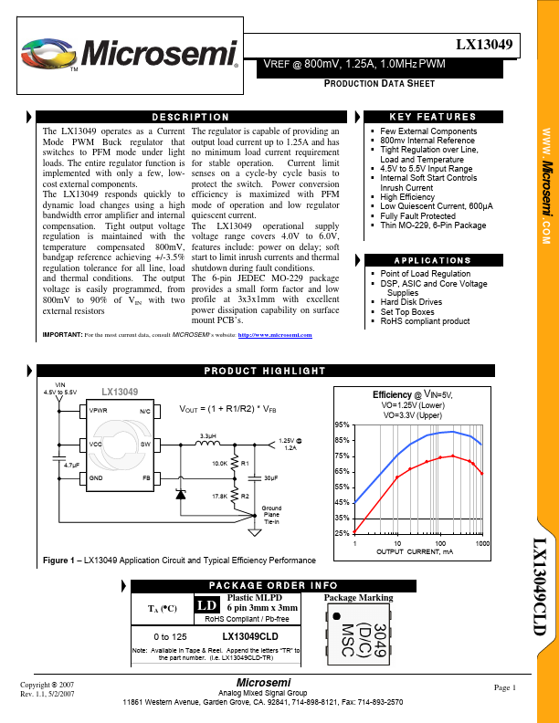
The LX13049 operates as a Current The regulator is capable of providing an
Mode PWM Buck regulator that output load current up to 1.25A and has
switches to PFM mode under light no minimum load current requirement
loads. The entire regulator function is for stable operation. Current limit
implemented with only a few, low- senses on a cycle-by cycle basis to
cost external components.
protect the switch. Power conversion
The LX13049 responds quickly to efficiency is maximized with PFM
dynamic load changes using a high mode of operation and low regulator
bandwidth error amplifier and internal quiescent current.
compensation. Tight output voltage The LX13049 operational supply
regulation is maintained with the voltage range covers 4.0V to 6.0V,
temperature compensated 800mV, features include: power on delay; soft
bandgap reference achieving +/-3.5% start to limit inrush currents and thermal
regulation tolerance for all line, load shutdown during fault conditions.
and thermal conditions. The output The 6-pin JEDEC MO-229 package
voltage is easily programmed, from provides a small form factor and low
800mV to 90% of VIN with two profile at 3x3x1mm with excellent
external resistors
power dissipation capability on surface
mount PCB’s.
IMPORTANT: For the most current data, consult MICROSEMI’s website: http://www.microsemi.com
KEY FEATURES
Few External Components
800mv Internal Reference
Tight Regulation over Line,
Load and Temperature
4.5V to 5.5V Input Range
Internal Soft Start Controls
Inrush Current
High Efficiency
Low Quiescent Current, 600μA
Fully Fault Protected
Thin MO-229, 6-Pin Package
APPLICATIONS
Point of Load Regulation
DSP, ASIC and Core Voltage
Supplies
Hard Disk Drives
Set Top Boxes
RoHS compliant product
VIN
4.5V to 5.5V
LX13049
VPWR
N/C
VCC Part SW
4.7µF
GND
FB
PRODUCT HIGHLIGHT
VOUT = (1 + R1/R2) * VFB
3.3µH
10.0K R1
1.25V @
1.2A
30µF
17.8K R2
Ground
Plane
Tie-in
95%
85%
75%
65%
55%
45%
35%
25%
1
Figure 1 – LX13049 Application Circuit and Typical Efficiency Performance
Efficiency @ VIN=5V,
VO=1.25V (Lower)
VO=3.3V (Upper)
10 100
OUTPUT CURRENT, mA
TA (°C)
PACKAGE ORDER INFO
Plastic MLPD
LD 6 pin 3mm x 3mm
Package Marking
RoHS Compliant / Pb-free
0 to 125
LX13049CLD
Note: Available in Tape & Reel. Append the letters “TR” to
the part number. (i.e. LX13049CLD-TR)
Copyright © 2007
Rev. 1.1, 5/2/2007
Microsemi
Analog Mixed Signal Group
11861 Western Avenue, Garden Grove, CA. 92841, 714-898-8121, Fax: 714-893-2570
1000
Page 1