1214GN-650V
DESCRIPTION
The 1214GN-650V is an internally matched, MON SOURCE, class AB Ga N on Si C HEMT transistor capable of providing over 17d B gain, 650 Watts of pulsed RF output power at 150μs pulse width, 10% duty cycle across the 1200 to 1400 MHz band. The transistor has internal pre-match for optimal performance. This hermetically sealed transistor can be used for Broadband Avionics Data Link applications. It utilizes gold metallization and eutectic attach to provide highest reliability and superior ruggedness.
ABSOLUTE MAXIMUM RATINGS
Maximum Power Dissipation Device Dissipation @ 25C 1300 W
Maximum Voltage and Current
Drain-Source Voltage (VDSS)
150 V
Gate-Source Voltage (VGS) -8 to +0 V
Maximum Temperatures
Storage Temperature (TSTG) -55 to +125 C Operating Junction Temperature +250 C
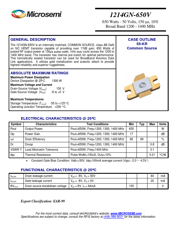
CASE OUTLINE 55-KR mon Source
ELECTRICAL CHARACTERISTICS @ 25C
Symbol
Characteristics
Pout
Output Power
Test Conditions
Min Typ Max Units
Pout=650W, Freq=1200, 1300, 1400 MHz 650
Gp...