Datasheet4U Logo Datasheet4U.com

MT4C16270 - DRAM 256K X 16 DRAM 5V / EDO PAGE MODE

Description

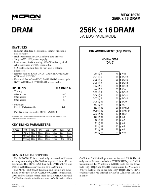
The MT4C16270 is a randomly accessed solid-state memory containing 4,194,304 bits organized in a x16 configuration.

The MT4C16270 has both BYTE WRITE and WORD WRITE access cycles via two CAS# pins.

Features

  • Industry-standard x16 pinouts, timing, functions and packages.
  • High-performance CMOS silicon-gate process.
  • Single +5V ±10% power supply.
  • Low power, 3mW standby; 300mW active, typical.
  • All device pins are TTL-compatible.
  • 512-cycle refresh in 8ms (9 row- and 9 column addresses).
  • Refresh modes: RAS#-ONLY, CAS#-BEFORE-RAS# (CBR) and HIDDEN.
  • Extended Data-Out (EDO) PAGE MODE access cycle.
  • BYTE WRITE and BYTE READ a.

📥 Download Datasheet

Datasheet preview – MT4C16270

Datasheet Details

Part number MT4C16270
Manufacturer Micron Technology
File Size 278.44 KB
Description DRAM 256K X 16 DRAM 5V / EDO PAGE MODE
Datasheet download datasheet MT4C16270 Datasheet
Additional preview pages of the MT4C16270 datasheet.
Other Datasheets by Micron Technology

Full PDF Text Transcription

Click to expand full text
TECHNOLOGY, INC. MT4C16270 256K x 16 DRAM DRAM FEATURES • Industry-standard x16 pinouts, timing, functions and packages • High-performance CMOS silicon-gate process • Single +5V ±10% power supply* • Low power, 3mW standby; 300mW active, typical • All device pins are TTL-compatible • 512-cycle refresh in 8ms (9 row- and 9 column addresses) • Refresh modes: RAS#-ONLY, CAS#-BEFORE-RAS# (CBR) and HIDDEN • Extended Data-Out (EDO) PAGE MODE access cycle • BYTE WRITE and BYTE READ access cycles 256K x 16 DRAM 5V, EDO PAGE MODE PIN ASSIGNMENT (Top View) 40-Pin SOJ (DA-6) OPTIONS • Timing 40ns access 50ns access 60ns access • Packages Plastic SOJ (400 mil) MARKING -4* -5* -6 DJ • Part Number Example: MT4C16270DJ-4 *40ns and 50ns access specifications are limited to a VCC range of ±5%.
Published: |