TC1302B Overview
Description
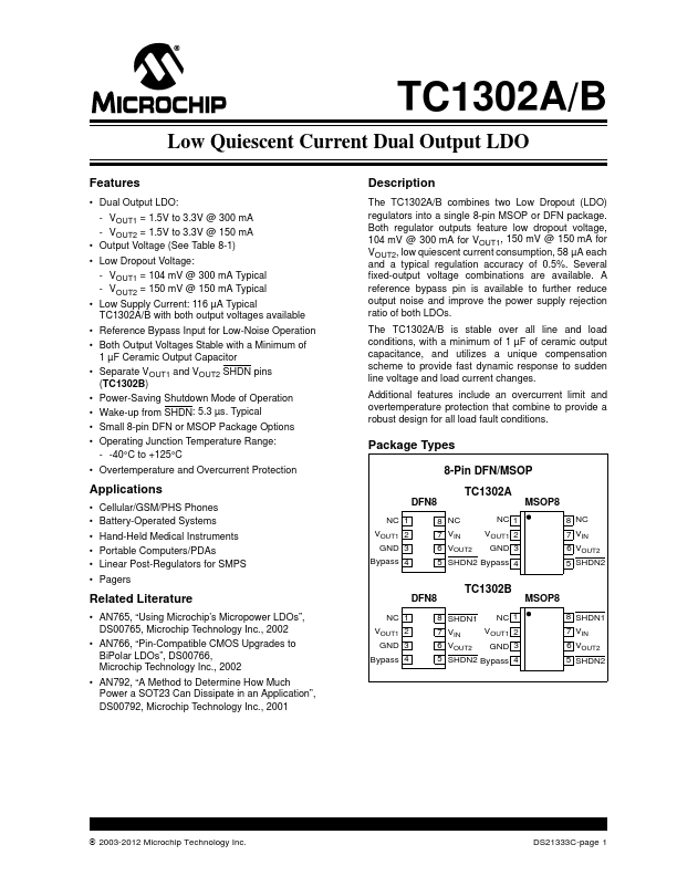
The TC1302A/B combines two Low Dropout (LDO) regulators into a single 8-pin MSOP or DFN package. Both regulator outputs feature low dropout voltage, 104 mV @ 300 mA for VOUT1, 150 mV @ 150 mA for VOUT2, low quiescent current consumption, 58 µA each and a typical regulation accuracy of 0.5%.
Key Features
- Dual Output LDO
- VOUT1 = 1.5V to 3.3V @ 300 mA
- VOUT2 = 1.5V to 3.3V @ 150 mA
- Output Voltage (See Table 8-1)
- Low Dropout Voltage
- VOUT1 = 104 mV @ 300 mA Typical
- VOUT2 = 150 mV @ 150 mA Typical
- Low Supply Current: 116 µA Typical TC1302A/B with both output voltages available
- Reference Bypass Input for Low-Noise Operation
- Both Output Voltages Stable with a Minimum of 1 µF Ceramic Output Capacitor