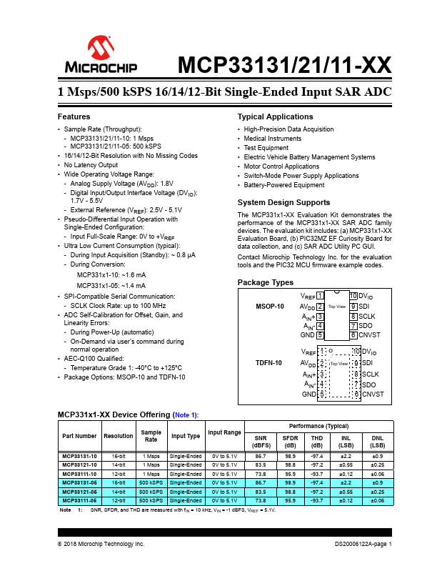
MCP33131/21/11-XX
Application Diagram
Analog Input
(0V to VREF)
Ground Reference of
Analog Input
2.5V to 5.1V 1.8V 1.7V to 5.5V
22Ω
VREF AVDD DVIO
1.7 nF
AIN+
MCP331x1-XX
SDI
CNVST
AIN-
SCLK
GND SDO
Host Device
(PIC32MZ)
Description
The MCP33131/MCP33121/MCP33111-10 and
MCP33131/MCP33121/MCP33111-05
are
single-ended 16, 14, and 12-bit, single-channel 1 Msps
and 500 kSPS ADC family devices, respectively,
featuring low power consumption and high
performance, using a successive approximation
register (SAR) architecture.
The device operates with a 2.5V to 5.1V external
reference (VREF), which supports a wide range of input
full-scale range from 0V to VREF. The reference voltage
setting is independent of the analog supply voltage
(AVDD) and is higher than AVDD. The conversion output
is available through an easy-to-use simple SPI-
compatible 3-wire interface.
The device requires a 1.8V analog supply voltage
(AVDD) and a 1.7V to 5.5V digital I/O interface supply
voltage (DVIO). The wide digital I/O interface supply
(DVIO) range (1.7V - 5.5V) allows the device to
interface with most host devices (Master) available in
the current industry such as the PIC32
microcontrollers, without using external voltage level
shifters.
When the device is first powered-up, it performs a
self-calibration to minimize offset, gain and linearity
errors. The device performance stays stable across the
specified temperature range. However, when extreme
changes in the operating environment, such as in the
reference voltage, are made with respect to the initial
conditions (e.g. the reference voltage was not fully
settled during the initial power-up sequence), the user
may send a recalibrate command anytime to initiate
another self-calibration to restore optimum
performance.
When the initial power-up sequence is completed, the
device enters a low-current input acquisition mode,
where sampling capacitors are connected to the input
pins. This mode is called Standby.
During Standby, most of the internal analog circuitry is
shutdown in order to reduce current consumption.
Typically, the device consumes less than 1 µA during
Standby. A new conversion is started on the rising edge
of CNVST. When the conversion is complete and the
host lowers CNVST, the output data is presented on
SDO, and the device enters Standby to begin acquiring
the next input sample. The user can clock out the ADC
output data using the SPI-compatible serial clock
during Standby.
The ADC system clock is generated by an internal
on-chip clock, therefore the conversion is performed
independent of the SPI serial clock (SCLK).
This device can be used for various high-speed and
high-accuracy analog-to-digital data conversion
applications, where design simplicity, low power, and
no output latency are needed.
The device is AEC-Q100 qualified for automotive
applications and operates over the extended
temperature range of -40°C to +125°C. The available
package options are Pb-free TDFN-10 and MSOP-10.
DS20006122A-page 2
2018 Microchip Technology Inc.