LLSD101C Overview
Key Specifications
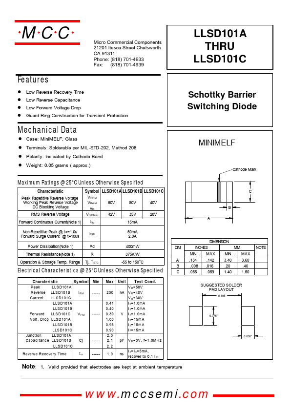
Mount Type: Surface Mount
Pins: 2
Height: 1.6 mm
Length: 3.7 mm
| Part | LLSD101C |
|---|---|
| Description | Schottky Barrier Switching Diode |
| Category | Diode |
| Manufacturer | Micro Commercial Components |
| Size | 360.06 KB |
Mount Type: Surface Mount
Pins: 2
Height: 1.6 mm
Length: 3.7 mm
| Seller | Inventory | Price Breaks | Buy |
|---|---|---|---|
| VNN Services | 3716 | 1+ : 2.27 USD 10+ : 2.23 USD 100+ : 2.19 USD 1000+ : 2.15 USD |
View Offer |
| Aztech | 1162 | 1+ : 15.11 USD | View Offer |
| Part Number | Manufacturer | Description |
|---|---|---|
| LLSD101C | Diodes Incorporated | SURFACE MOUNT SCHOTTKY BARRIER DIODE |
| LLSD101A | Diodes Incorporated | SURFACE MOUNT SCHOTTKY BARRIER DIODE |
| LLSD101B | Diodes Incorporated | SURFACE MOUNT SCHOTTKY BARRIER DIODE |
| LLSD101 | Diodes Incorporated | SURFACE MOUNT SCHOTTKY BARRIER DIODE |
| LLSD103A | Diodes Incorporated | SURFACE MOUNT SCHOTTKY BARRIER DIODE |