(Preliminary )P L 5 0 0 -3 7
Low Phase Noise VCXO (36MHz to 130MHz)
FE AT UR E S
VCXO output for the 36MHz to 130MHz range
Low phase noise (-148 dBc @ 10kHz offset at
77.76MHz).
CMOS output with OE tri-state control.
36 to 130MHz fundamental crystal input.
Integrated high linearity variable capacitors.
8mA drive capability at TTL output.
+/- 150 ppm pull range, max 5% linearity.
Low jitter (RMS): 2.5ps period jitter.
Single 2.5V ±10% or 3.3V ±10 power supply.
Operating temperature range from -40C to +85C
Available in Die or Wafer form or SOP-8L or
SOT23-6L packaging.
PIN AND PAD CONFIGURATION
XIN
OE^
VCON
GND
18
27
36
45
SOP-8L
XOUT
DNC
VDD
CLK
VCON
GND
XIN
1
2
3
6 CLK
5 VDD
4 XOUT
DESCRIPTION
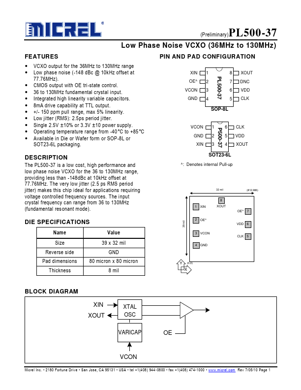
The PL500-37 is a low cost, high performance and
low phase noise VCXO for the 36 to 130MHz range,
providing less than -148dBc at 10kHz offset at
77.76MHz. The very low jitter (2.5 ps RMS period
jitter) makes this chip ideal for applications requiring
voltage controlled frequency sources. The input
crystal frequency can range from 36 to 130MHz
(fundamental resonant mode).
DIE SPECIFICATIONS
Name
Value
Size
Reverse side
Pad dimensions
Thickness
39 x 32 mil
GND
80 micron x 80 micron
8 mil
SOT23-6L
^: Denotes internal Pull-up
1 XIN
32 mil
8
XOUT
2 OE^
3 VCON
4 GND
(812,986)
OE^ 7
VDD 6
CLK 5
Y (0,0)
X
BLOCK DIAGRAM
XIN
XOUT
XTAL
OSC
VARICAP
OE
VCON
Micrel Inc. • 2180 Fortune Drive • San Jose, CA 95131 • USA • tel +1(408) 944 -0800 • fax +1(408) 474-1000 • www.micrel.com Rev 7/05/10 Page 1