PL500-17
Low Phase Noise VCXO (17MHz to 36MHz)
FE AT UR E S
PIN CONFIGURATION
VCXO output for the 17MHz to 36MHz range
Low phase noise (-130dBc @ 10kHz offset at
35.328MHz)
LVCMOS output with OE tri-state control
17 to 36MHz fundamental crystal input
Integrated high linearity variable capacitors
8mA drive capability at TTL output
±150 ppm pull range, max 5% (typ.) linearity
Low jitter (RMS): 2.5ps period jitter
2.5 to 3.3V operation
Available in 8-Pin SOP, 6-pin SOT23 GREEN/
RoHS compliant packages, or Die
DESCRIPTION
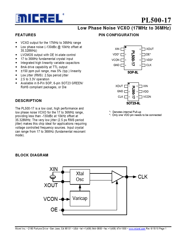
The PL500-17 is a low cost, high performance and
low phase noise VCXO for the 17 to 36MHz range,
providing less than -130dBc at 10kHz offset at
35.328MHz. The very low jitter (2.5 ps RMS period
jitter) makes this chip ideal for applications requiring
voltage controlled frequency sources. Input crystal
can range from 17 to 36MHz (fundamental resonant
mode).
XIN
VDD*
VCON
GND
18
27
36
45
SOP-8L
XOUT
OE^
VDD*
CLK
XOUT
GND
CLK
1
2
3
6 XIN
5 VDD
4 VCON
SOT23-6L
^: Denotes internal Pull-up
*: Only one VDD pin needs to be connected
BLOCK DIAGRAM
XIN
XOUT
VCON
OE
Xtal
Osc
Varicap
CLK
Micrel Inc. • 2180 Fortune Drive • San Jose, CA 95131 • USA • tel +1(408) 944-0800 • fax +1(408) 474-1000 • www.micrel.com Rev 6/15/10 Page 1