PL502-03
PL502-03 is Low Phase Noise VCXO manufactured by Micrel Semiconductor.
Low Phase Noise VCXO (48MHz to 100MHz)
FE AT UR E S
- VCXO output for the 48MHz to 100MHz range
- Low phase noise (-130 dBc @ 10kHz offset at
48MHz)
- LVCMOS output
- 12 to 25MHz crystal input
- Integrated variable capacitors
- Selectable High Drive (30mA) or Standard Drive
(10mA) output
- Wide pull range (± 250 ppm typ)
- Low period jitter: 3.5ps RMS
- 3.3V operation
- Available in 8-Pin SOP
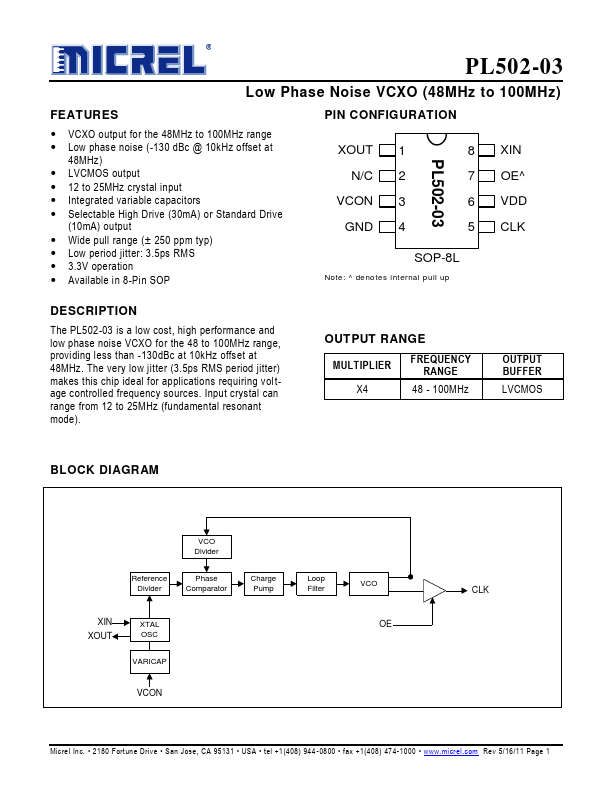
PIN CONFIGURATION
XOUT N/C
VCON GND
1 2 3 4
8 7 6 5
SOP-8L
Note: ^ denotes internal pull up
XIN OE^ VDD CLK
DESCRIPTION
The PL502-03 is a low cost, high performance and low phase noise VCXO for the 48 to 100MHz range, providing less than -130dBc at 10kHz offset at 48MHz....