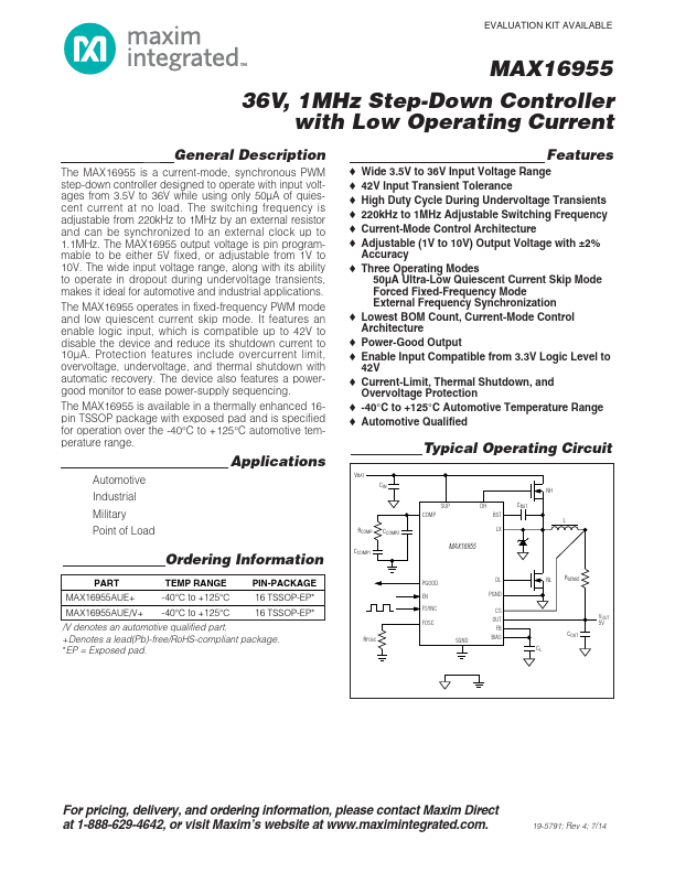
MAX16955
36V, 1MHz Step-Down Controller
with Low Operating Current
ABSOLUTE MAXIMUM RATINGS
SUP and EN to SGND ............................................-0.3V to +42V
LX to PGND ..............................................................-1V to +42V
BST to LX .................................................................-0.3V to +6V
BIAS, FB, PGOOD, FSYNC to SGND .......................-0.3V to +6V
DH to LX ...................................................................-0.3V to +6V
DL to PGND .............................................-0.3V to (VBIAS + 0.3V)
FOSC to SGND ........................................-0.3V to (VBIAS + 0.3V)
CS and OUT to SGND ............................................-0.3V to +11V
PGND to SGND .....................................................-0.3V to +0.3V
Continuous Power Dissipation (TA = +70°C)
TSSOP (derate 26.1mW/°C above +70°C) .............2088.8mW*
Operating Temperature Range .........................-40°C to +125°C
Junction Temperature ......................................................+150°C
Storage Temperature Range .............................-65°C to +150°C
Lead Temperature (soldering, 10s) .................................+300°C
Soldering Temperature (reflow) .......................................+260°C
*As per JEDEC51 standard (multilayer board).
Stresses beyond those listed under “Absolute Maximum Ratings” may cause permanent damage to the device. These are stress ratings only, and functional
operation of the device at these or any other conditions beyond those indicated in the operational sections of the specifications is not implied. Exposure to
absolute maximum rating conditions for extended periods may affect device reliability.
PACKAGE THERMAL CHARACTERISTICS (Note 1)
TSSOP
Junction-to-Ambient Thermal Resistance (θJA) .........38.3°C/W
Junction-to-Case Thermal Resistance (θJC) ...................3°C/W
Note 1: Package thermal resistances were obtained using the method described in JEDEC specification JESD51-7, using a four-layer
board. For detailed information on package thermal considerations, refer to www.maximintegrated.com/thermal-tutorial.
ELECTRICAL CHARACTERISTICS
(VSUP = VEN = 14V, CIN = 10μF, COUT = 94μF, CBIAS = 2.2μF, CBST = 0.1μF, RFOSC = 76.8kΩ, TA = TJ = -40°C to +125°C, unless
otherwise noted. Typical values are at TA = +25°C.) (Note 2)
PARAMETER
SYMBOL
CONDITIONS
MIN TYP MAX UNITS
SUP Input Voltage Range
SUP Operating Supply Current
Skip Mode Supply Current
SUP Shutdown Supply Current
BIAS Voltage
BIAS Undervoltage Lockout
Hysteresis
VSUP
ISUP
ISKIP
ISHDN,SUP
VBIAS
VUVBIAS
(Note 3)
Fixed 5V output, fixed-frequency, PWM
mode, VFB = VBIAS, no external FETs
connected
No load, fixed 5V output
VEN = 0V
VSUP = 3.5V, IBIAS = 45mA
6V < VSUP < 36V
VBIAS rising
VBIAS falling
3.5 36 V
1 mA
50 90 μA
10 20 μA
3.0
4.7 5.0 5.3
V
3.1 3.4
V
200 mV
BIAS Minimum Load
OUTPUT VOLTAGE (OUT)
IBIAS(MIN) VSUP - VBIAS > 200mV
45 mA
Output Voltage Adjustable
Range
1.0 10 V
OUT Pulldown Resistance
Output Voltage (5V Fixed Mode)
RPULL_D
VOUT
VEN = 0V or fault condition active
VSUP = 6V to 36V, VFB = VBIAS, fixed-
frequency mode (Note 4)
30
4.925 5.0 5.075
V
FB Feedback Voltage
(Adjustable Mode)
VFB
VSUP = 6V to 36V, 0V < (VCS - VOUT)
< 80mV, fixed-frequency mode
0.99 1.0 1.01
V
FB Current
IFB VFB = 1.0V
0.02
μA
2 Maxim Integrated