DS3502 Overview
Key Specifications
Mount Type: Screw
Description
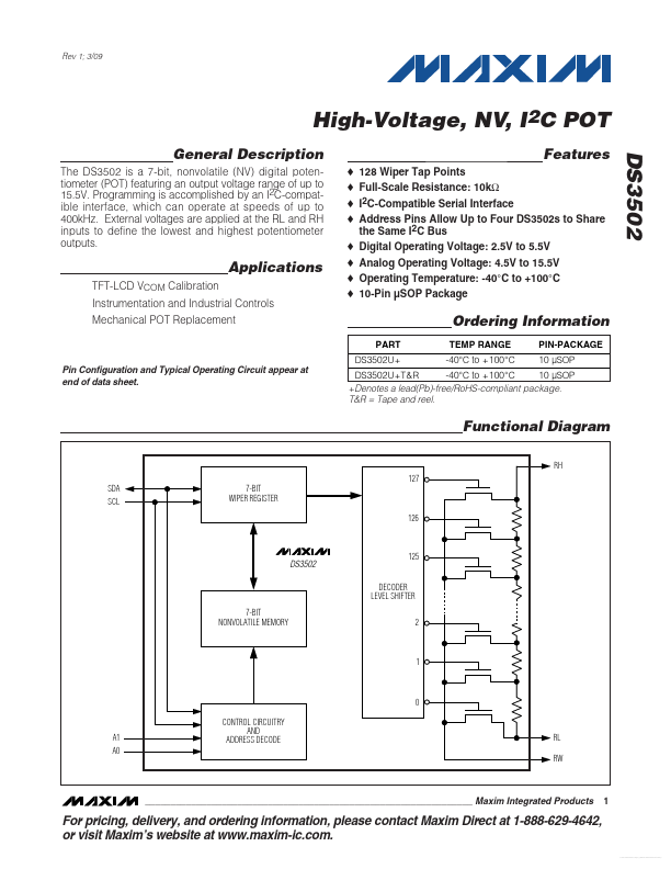
The DS3502 is a 7-bit, nonvolatile (NV) digital potentiometer (POT) featuring an output voltage range of up to 15.5V. Programming is accomplished by an I2C-compatible interface, which can operate at speeds of up to 400kHz.
Key Features
- Address Pins Allow Up to Four DS3502s to Share the Same I2C Bus
- Digital Operating Voltage: 2.5V to 5.5V
- Analog Operating Voltage: 4.5V to 15.5V
- Operating Temperature: -40°C to +100°C
- 10-Pin µSOP Package