ME15N10-G
DESCRIPTION
ME15N10/ME15N10-G
FEATURES
- RDS(ON)≦100mΩ@VGS=10V
- Super high density cell design for extremely low RDS(ON)
- Exceptional on-resistance and maximum DC current capability
The ME15N10 is the N-Channel logic enhancement mode power field effect transistors, using high cell density, DMOS trench technology. This high density process is especially tailored to minimize on state resistance. These devices are particularly suited for low voltage application such as cellular phone, notebook puter power management and other battery powered circuits, and low in-line power loss that are needed in a very small outline surface mount package.
APPLICATIONS
- Power Management in Note book
- DC/DC Converter
- Load Switch
- LCD Display inverter
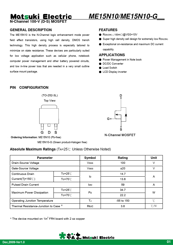
CONFIGURATION
(TO-252-3L) Top View e Ordering Information: ME15N10 (Pb-free)
ME15N10-G (Green product-Halogen free)
Absolute Maximum Ratings (TA=25℃ Unless Otherwise Noted)
Parameter
Drain-Source Voltage Gate-Source Voltage Continuous Drain...