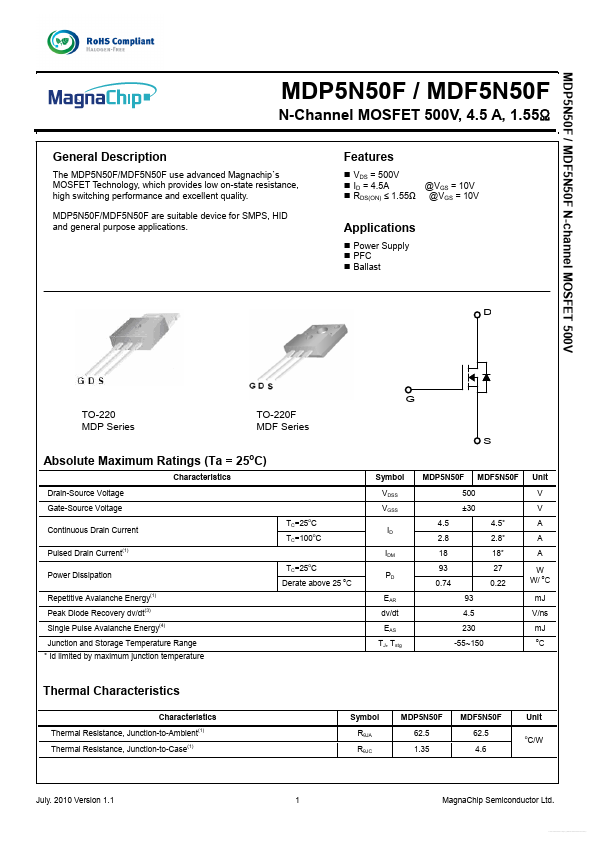
Ordering Information
Part Number
MDP5N50FTH
MDF5N50FTH
Temp. Range
-55~150oC
-55~150oC
Package
TO-220
TO-220F
Packing
Tube
Tube
RoHS Status
Halogen Free
Halogen Free
Electrical Characteristics (Ta =25oC)
Characteristics
Symbol
Static Characteristics
Drain-Source Breakdown Voltage
Gate Threshold Voltage
Drain Cut-Off Current
Gate Leakage Current
Drain-Source ON Resistance
Forward Transconductance
Dynamic Characteristics
BVDSS
VGS(th)
IDSS
IGSS
RDS(ON)
gfs
Total Gate Charge
Qg
Gate-Source Charge
Qgs
Gate-Drain Charge
Qgd
Input Capacitance
Ciss
Reverse Transfer Capacitance
Crss
Output Capacitance
Coss
Turn-On Delay Time
td(on)
Rise Time
tr
Turn-Off Delay Time
td(off)
Fall Time
tf
Drain-Source Body Diode Characteristics
Maximum Continuous Drain to
Source Diode Forward Current
Source-Drain Diode Forward
Voltage
Body Diode Reverse Recovery
Time
Body Diode Reverse Recovery
Charge
IS
VSD
trr
Qrr
Test Condition
ID = 250µA, VGS = 0V
VDS = VGS, ID = 250µA
VDS = 500V, VGS = 0V
VGS = ±20V, VDS = 0V
VGS = 10V, ID = 2.5A
VDS = 30V, ID = 2.5A
VDS = 500V, ID = 5.0A, VGS = 10V(3)
VDS = 25V, VGS = 0V, f = 1.0MHz
VGS = 10V, VDS = 250V, ID = 5.0A,
RG = 25Ω(3)
IS = 5.0A, VGS = 0V
IF = 5.0A, dl/dt = 100A/µs(3)
Min Typ Max Unit
500 -
2.5 -
-
V
4.5
- - 10 µA
- - 100 uA
1.25 1.55
Ω
-
3.3 -
S
- 12.1 15.73
- 3.6 - nC
- 4.3 -
- 500 650
- 1.5 2.25 pF
- 65 84.5
- 23 48.3
- 30 60
ns
- 37 77.7
- 29 60.9
- 4.5 - A
- 1.4 V
- 80
ns
- 1.6
µC
Note :
1. Pulse width is based on R θJC & R θJA and the maximum allowed junction temperature of 150°C.
2. Pulse test: pulse width ≤300us, duty cycle≤2%, pulse width limited by junction temperature TJ(MAX)=150°C.
3. ISD ≤4.5A, di/dt≤200A/us, VDD=50V, Rg =25Ω, Starting TJ=25°C
4. L=20.5mH, IAS=4.5A, VDD=50V, , Rg =25Ω, Starting TJ=25°C
July. 2010 Version 1.1
2 MagnaChip Semiconductor Ltd.
Free Datasheet http://www.datasheet4u.com/