MX29SL402CT Overview
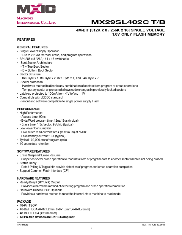
MX29SL402C T/B 4M-BIT [512K x 8 / 256K x 16] SINGLE VOLTAGE 1.8V ONLY FLASH MEMORY.
MX29SL402CT Key Features
- Single Power Supply Operation
- 1.65 to 2.2 volt for read, erase, and program operations
- 524,288 x 8 / 262,144 x 16 switchable
- Boot Sector Architecture
- T = Top Boot Sector
- B = Bottom Boot Sector
- Sector Structure
- Sector protection
- Hardware method to disable any bination of sectors from program or erase operations
- Temporary sector unprotected allows code changes in previously locked sectors


