Description
The PXAD184218FV is a 420-watt (P3dB) LDMOS FET with an asymmetrical design intended for use in multi-standard cellular power amplifier applications in the 1805 to 1880 MHz frequency band.
Features
- include dual-path design, input and output matching, high gain and thermally-enhanced package with earless flanges. Manufactured with an advanded LDMOS process, this device provides excellent thermal performance and superior reliability. PXAD184218FV Package H-37275G-6/2
Peak/Average Ratio, Gain (dB) Efficiency (%)
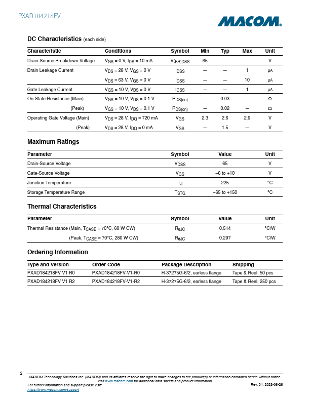
Single-carrier WCDMA Drive-up
VDD = 28 V, IDQ(MAIN) = 720 mA, VGS(PEAK) = 1.4 V, ƒ = 1880 MHz,
3GPP WCDMA signal, PAR = 10 dB,
3.84 MHz BW
24
60
Efficiency
20
40
16
20
1.
 PXAD184218FV Datasheet