LTC6957-4
Features n Low Phase Noise Buffer/Driver n Optimized Conversion of Sine Wave Signals to
Logic Levels n Three Logic Output Types Available
- LVPECL
- LVDS
- CMOS n Additive Jitter 45fs RMS (LTC6957-1) n Frequency Range Up to 300MHz n3.15V to 3.45V Supply Operation n Low Skew 3ps Typical n Fully Specified from
- 40°C to 125°C n12-Lead MSOP and 3mm × 3mm DFN Packages
Applications n System Reference Frequency Distribution n High Speed ADC, DAC, DDS Clock Driver n Military and Secure Radio n Low Noise Timing Trigger n Broadband Wireless Transceiver n High Speed Data Acquisition n Medical Imaging n Test and Measurement
LTC6957-1/LTC6957-2/ LTC6957-3/LTC6957-4 Low Phase Noise, Dual Output Buffer/Driver/
Logic Converter Description
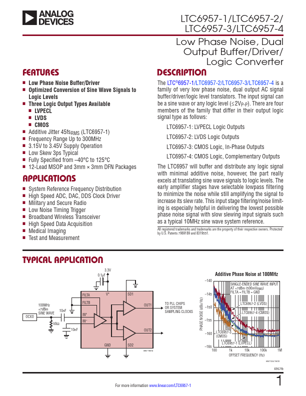
The LTC®6957-1/LTC6957-2/LTC6957-3/LTC6957-4 is a family of very low phase noise, dual output AC signal buffer/driver/logic level translators. The input signal can be a sine wave or any logic level (≤2VP-P). There are four members of the family...