Datasheet4U Logo Datasheet4U.com
Lattice Semiconductor logo

ispClock5410D Datasheet

Manufacturer: Lattice Semiconductor
ispClock5410D datasheet preview

Datasheet Details

Part number ispClock5410D
Datasheet ispClock5410D_LatticeSemiconductor.pdf
File Size 2.02 MB
Manufacturer Lattice Semiconductor
Description Zero Delay And Fan-Out Buffer
ispClock5410D page 2 ispClock5410D page 3

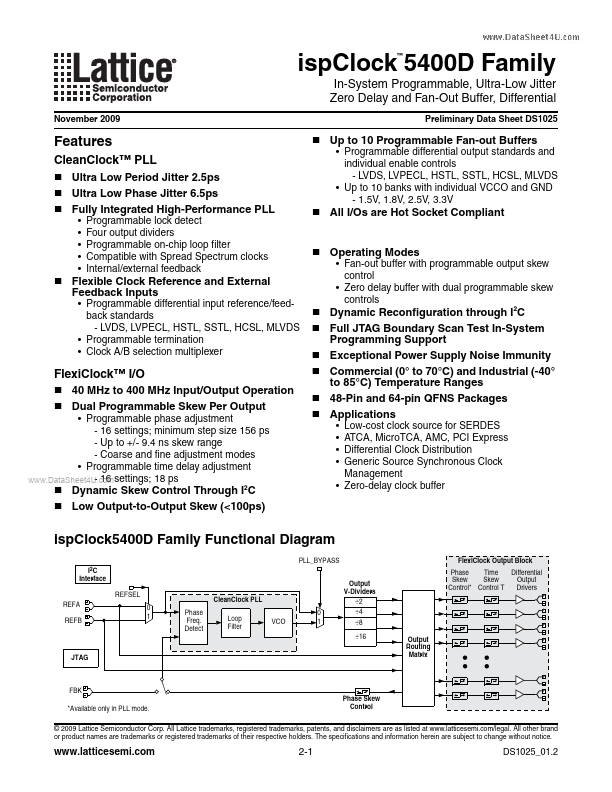
ispClock5410D Overview

The ispClock5400D family integrates a CleanClock PLL and a FlexiClock Output block. The CleanClock PLL provides an ultra-low-jitter clock source to a set of four V-dividers. The FlexiClock output block receives the clock output from these V-dividers through an output switch matrix and distributes them.

ispClock5410D Key Features

  • Ultra Low Period Jitter 2.5ps
  • Ultra Low Phase Jitter 6.5ps
  • Fully Integrated High-Performance PLL
  • Programmable lock detect Four output dividers Programmable on-chip loop filter patible with Spread Spectrum clocks Inter
  • Up to 10 Programmable Fan-out Buffers
  • Programmable differential output standards and individual enable controls
  • LVDS, LVPECL, HSTL, SSTL, HCSL, MLVDS
  • Up to 10 banks with individual VCCO and GND
  • 1.5V, 1.8V, 2.5V, 3.3V
  • All I/Os are Hot Socket pliant
Lattice Semiconductor logo - Manufacturer

More Datasheets from Lattice Semiconductor

See all Lattice Semiconductor datasheets

Part Number Description
ispClock5400D Zero Delay And Fan-Out Buffer
ispClock5406D Zero Delay And Fan-Out Buffer
ISPCLOCK5300S In-System Programmable Zero-Delay
ISPCLOCK5304S In-System Programmable Zero-Delay
ISPCLOCK5308S In-System Programmable Zero-Delay
ISPCLOCK5312S In-System Programmable Zero-Delay
ISPCLOCK5316S In-System Programmable Zero-Delay
ISPCLOCK5320S In-System Programmable Zero-Delay
ISPCLOCK5500 In-System Programmable Zero-Delay
ISPCLOCK5510 In-System Programmable Zero-Delay

ispClock5410D Distributor

Datasheet4U Logo
Since 2006. D4U Semicon. About Datasheet4U Contact Us Privacy Policy Purchase of parts