ispClock™5400D Family
In-System Programmable, Ultra-Low Jitter
Zero Delay and Fan-Out Buffer, Differential
November 2009
Preliminary Data Sheet DS1025
Features
CleanClock™ PLL
Ultra Low Period Jitter 2.5ps
Ultra Low Phase Jitter 6.5ps
Fully Integrated High-Performance PLL
• Programmable lock detect
• Four output dividers
• Programmable on-chip loop filter
• Compatible with Spread Spectrum clocks
• Internal/external feedback
Flexible Clock Reference and External
Feedback Inputs
• Programmable differential input reference/feed-
back standards
- LVDS, LVPECL, HSTL, SSTL, HCSL, MLVDS
• Programmable termination
• Clock A/B selection multiplexer
FlexiClock™ I/O
40 MHz to 400 MHz Input/Output Operation
Dual Programmable Skew Per Output
• Programmable phase adjustment
- 16 settings; minimum step size 156 ps
- Up to +/- 9.4 ns skew range
- Coarse and fine adjustment modes
• Programmable time delay adjustment
www.DataSheet4U-.c1o6msettings; 18 ps
Dynamic Skew Control Through I2C
Low Output-to-Output Skew (<100ps)
Up to 10 Programmable Fan-out Buffers
• Programmable differential output standards and
individual enable controls
- LVDS, LVPECL, HSTL, SSTL, HCSL, MLVDS
• Up to 10 banks with individual VCCO and GND
- 1.5V, 1.8V, 2.5V, 3.3V
All I/Os are Hot Socket Compliant
Operating Modes
• Fan-out buffer with programmable output skew
control
• Zero delay buffer with dual programmable skew
controls
Dynamic Reconfiguration through I2C
Full JTAG Boundary Scan Test In-System
Programming Support
Exceptional Power Supply Noise Immunity
Commercial (0° to 70°C) and Industrial (-40°
to 85°C) Temperature Ranges
48-Pin and 64-pin QFNS Packages
Applications
• Low-cost clock source for SERDES
• ATCA, MicroTCA, AMC, PCI Express
• Differential Clock Distribution
• Generic Source Synchronous Clock
Management
• Zero-delay clock buffer
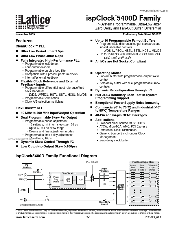
ispClock5400D Family Functional Diagram
I2C
Interface
REFA
REFB
REFSEL
0
1
JTAG
FBK
*Available only in PLL mode.
PLL_BYPASS
Phase
Freq.
Detect
CleanClock PLL
Loop
Filter
VCO
Output
V-Dividers
÷2
0 ÷4
1 ÷8
÷16
Phase Skew
Control
Output
Routing
Matrix
FlexiClock Output Block
Phase
Skew
Control*
Time
Skew
Control T
Differential
Output
Drivers
+
+
+
+
+
+
© 2009 Lattice Semiconductor Corp. All Lattice trademarks, registered trademarks, patents, and disclaimers are as listed at www.latticesemi.com/legal. All other brand
or product names are trademarks or registered trademarks of their respective holders. The specifications and information herein are subject to change without notice.
www.latticesemi.com
2-1
DS1025_01.2