Click to expand full text
Switching Diode
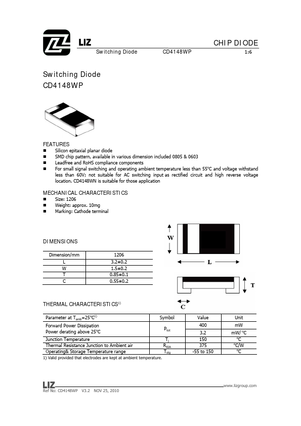
Switching Diode CD4148WP
CD4148WP
CHIP DIODE
1:6
FEATURES
Silicon epitaxial planar diode SMD chip pattern, available in various dimension included 0805 & 0603 Leadfree and RoHS compliance components For small signal switching and operating ambient temperature less than 55oC and voltage withstand
less than 60V; not suitable for AC switching input as rectified circuit and high reverse voltage location. CD4148WN is suitable for those application
MECHANICAL CHARACTERISTICS
Size: 1206 Weight: approx. 10mg Marking: Cathode terminal
DIMENSIONS
Dimension/mm L W T C
1206
3.2±0.2 1.5±0.2 0.85±0.1 0.55±0.
 CD4148WP Datasheet