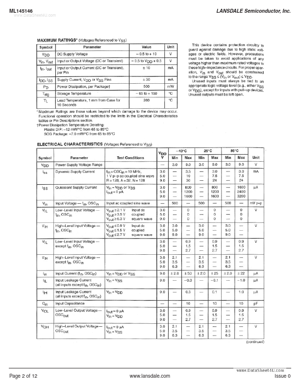
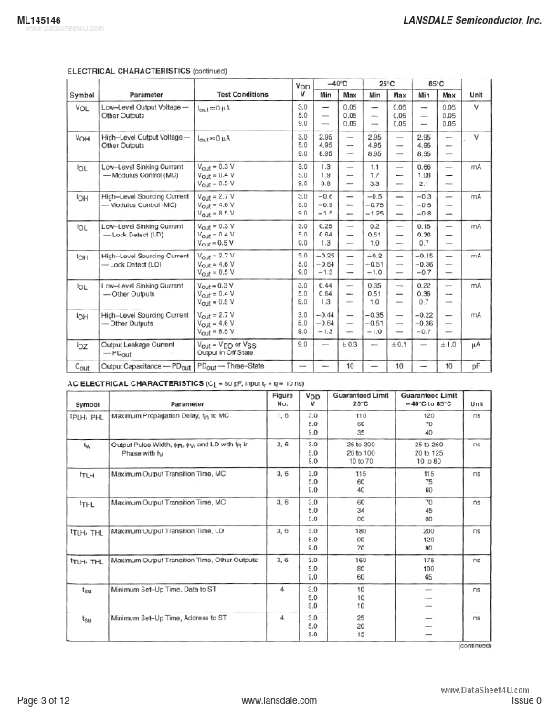
ML145146 Description
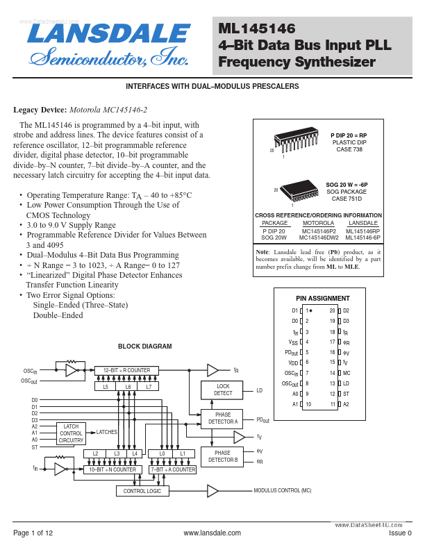
ML145146 4 Bit Data Bus Input PLL Frequency Synthesizer INTERFACES WITH DUAL MODULUS PRESCALERS Legacy Device: Motorola MC145146-2 The ML145146 is programmed by a 4 bit input, with strobe and address lines.
ML145146 Key Features
- Operating Temperature Range: TA
- 40 to +85°C
- Low Power Consumption Through the Use of CMOS Technology
- 3.0 to 9.0 V Supply Range
- Programmable Reference Divider for Values Between 3 and 4095
- Dual-Modulus 4-Bit Data Bus Programming
- ÷ N Range = 3 to 1023, ÷ A Range= 0 to 127
- Two Error Signal Options: Single-Ended (Three-State) Double-Ended
- logic levels) DC coupling may be used. OSCin/OSCout Reference Oscillator Input/Output (Pins 7 and 8) These pins form an