The following content is an automatically extracted verbatim text
from the original manufacturer datasheet and is provided for reference purposes only.
View original datasheet text
SMD Type
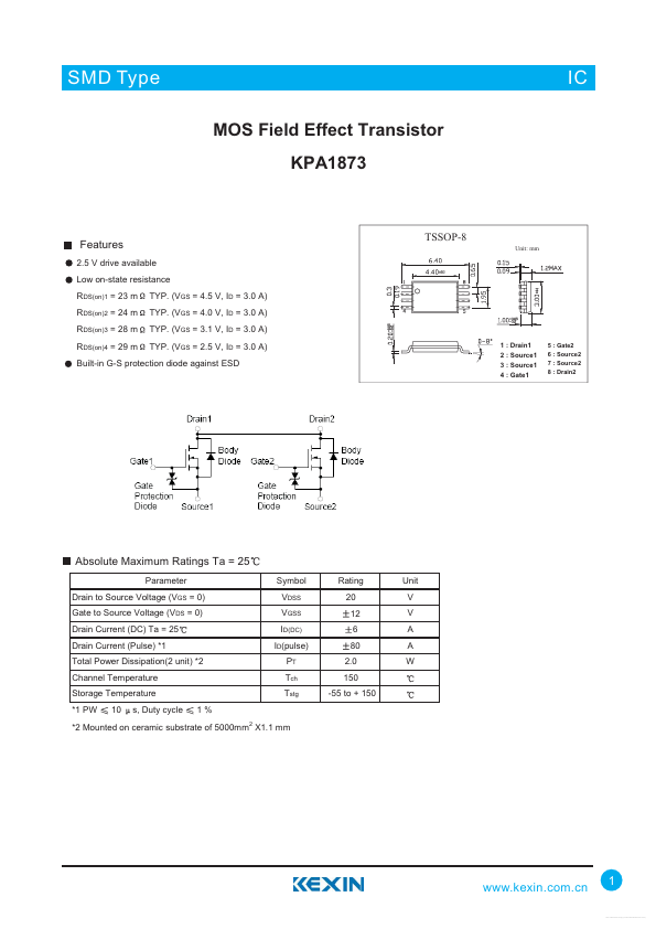
MOS Field Effect Transistor KPA1873
IC IC
Features
2.5 V drive available Low on-state resistance RDS(on)1 = 23 m RDS(on)2 = 24 m RDS(on)3 = 28 m RDS(on)4 = 29 m TYP. (VGS = 4.5 V, ID = 3.0 A) TYP. (VGS = 4.0 V, ID = 3.0 A) TYP. (VGS = 3.1 V, ID = 3.0 A) TYP. (VGS = 2.5 V, ID = 3.0 A)
TSSOP-8
Unit: mm
Built-in G-S protection diode against ESD
1 : Drain1 2 : Source1 3 : Source1 4 : Gate1
5 : Gate2 6 : Source2 7 : Source2 8 : Drain2
Absolute Maximum Ratings Ta = 25
Parameter Drain to Source Voltage (VGS = 0) Gate to Source Voltage (VDS = 0) Drain Current (DC) Ta = 25 Drain Current (Pulse) *1 Total Power Dissipation(2 unit) *2 Channel Temperature Storage Temperature *1 PW 10 s, Duty cycle 1% Symbol VDSS VGSS ID(DC) ID(pulse) PT Tch Tstg Rating 20 12 6 80 2.
 KPA1873 Datasheet