The following content is an automatically extracted verbatim text
from the original manufacturer datasheet and is provided for reference purposes only.
View original datasheet text
SMD Type
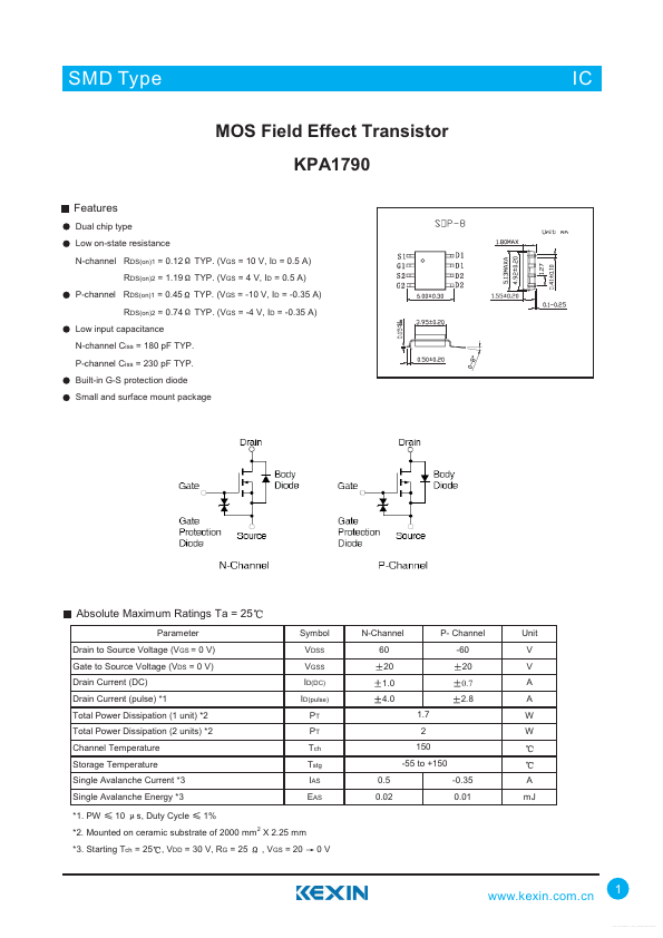
MOS Field Effect Transistor KPA1790
Features
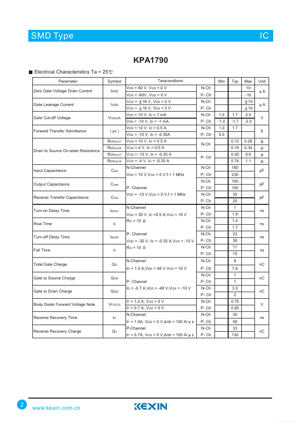
Dual chip type Low on-state resistance N-channel RDS(on)1 = 0.12 RDS(on)2 = 1.19 P-channel RDS(on)1 = 0.45 RDS(on)2 = 0.74 Low input capacitance N-channel Ciss = 180 pF TYP. P-channel Ciss = 230 pF TYP. Built-in G-S protection diode Small and surface mount package TYP. (VGS = 10 V, ID = 0.5 A) TYP. (VGS = 4 V, ID = 0.5 A) TYP. (VGS = -10 V, ID = -0.35 A) TYP. (VGS = -4 V, ID = -0.35 A)
IC IC
Absolute Maximum Ratings Ta = 25
Parameter Drain to Source Voltage (VGS = 0 V) Gate to Source Voltage (VDS = 0 V) Drain Current (DC) Drain Current (pulse) *1 Total Power Dissipation (1 unit) *2 Total Power Dissipation (2 units) *2 Channel Temperature Storage Temperature Single Avalanche Current *3 Single Avalanche Energy *3 *1.
 KPA1790 Datasheet