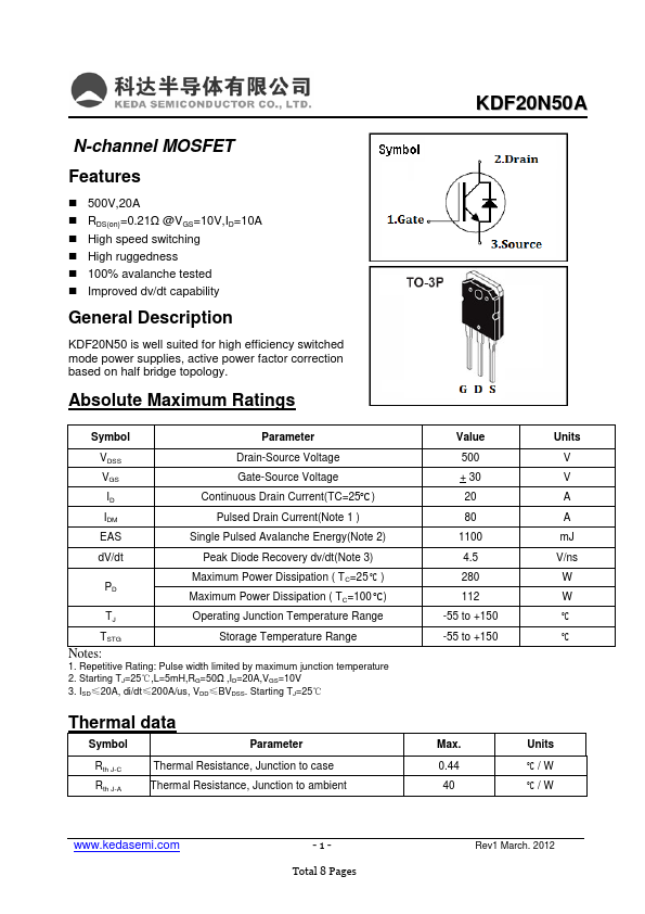
KDF20N50A Description
KDF20N50 is well suited for high efficiency switched mode power supplies, active power factor correction based on half bridge topology. Ratings Symbol Parameter VDSS VGS ID IDM EAS Drain-Source Voltage Gate-Source Voltage Continuous Drain Current(TC=25℃ ) Pulsed Drain Current(Note 1 ) Single Pulsed Avalanche Energy(Note 2) dV/dt Peak Diode Recovery dv/dt(Note 3) Maximum Power Dissipation ( TC=25 ℃ ) PD Maximum Power...
KDF20N50A Key Features
- 500V,20A
- RDS(on)=0.21Ω @VGS=10V,ID=10A
- High speed switching
- High ruggedness
- 100% avalanche tested
- Improved dv/dt capability