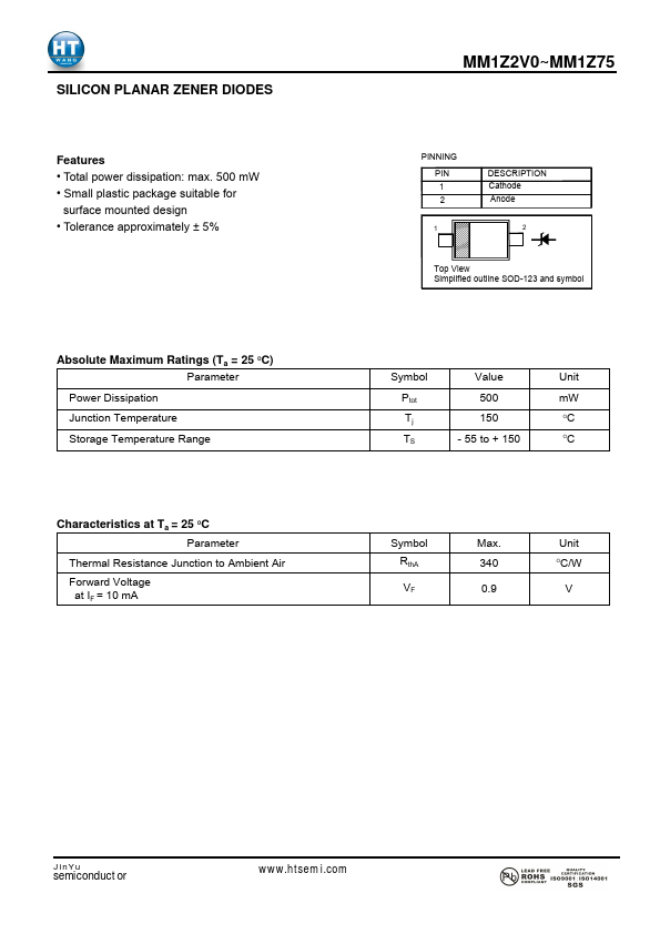
Small plastic package suitable for
surface mounted design.
Tolerance approximately ± 5%
Absolute Maximum Ratings (Ta = 25 OC) Parameter
Power Dissipation Junction Temperature Storage Temperature Range
Characteristics at Ta = 25 OC Parameter
Thermal Resistance Junction to Ambient Air Forward Voltage at IF = 10 mA
MM1Z2V0~MM1Z75.
The following content is an automatically extracted verbatim text
from the original manufacturer datasheet and is provided for reference purposes only.
View original datasheet text
SILICON PLANAR ZENER DIODES
Features • Total power dissipation: max. 500 mW • Small plastic package suitable for
surface mounted design • Tolerance approximately ± 5%
Absolute Maximum Ratings (Ta = 25 OC) Parameter
Power Dissipation Junction Temperature Storage Temperature Range
Characteristics at Ta = 25 OC Parameter
Thermal Resistance Junction to Ambient Air Forward Voltage at IF = 10 mA
MM1Z2V0~MM1Z75
PINNING PIN 1 2
1
DESCRIPTION Cathode Anode
2
Top View Simplified outline SOD-123 and symbol
Symbol Ptot Tj TS
Value 500 150 - 55 to + 150
Unit mW OC OC
Symbol RthA
VF
Max. 340
0.9
Unit OC/W
V
JinYu
semiconductor
www.htsemi.com
MM1Z2V0~MM1Z75
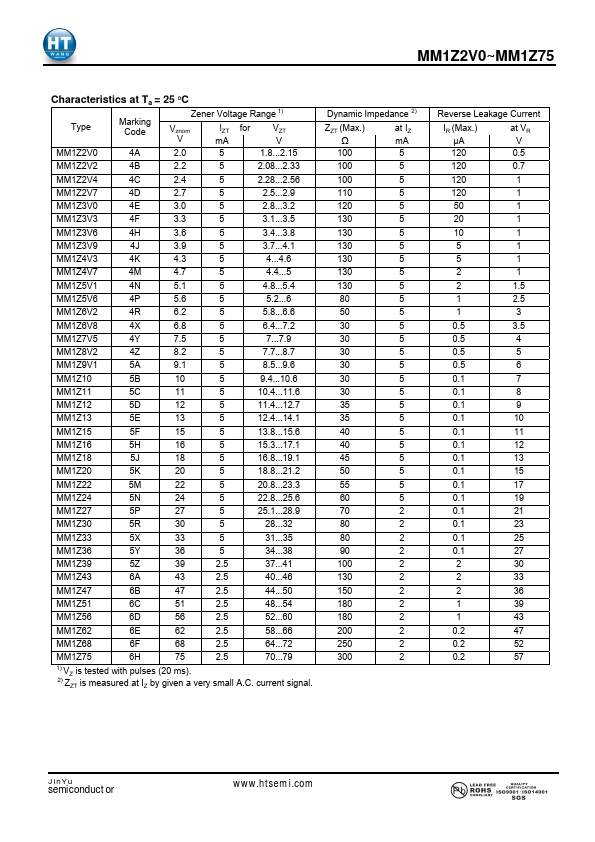
Characteristics at Ta = 25 OC
Type
Marking Code
Zener Voltage Range 1)
Vznom V
lZT for mA
VZT V
MM1Z2V0
4A
2.0
5
1.8...2.
 MM1Z2V0 Datasheet