Two DTC123JCA chips in a package
Marking: G11
Absolute maximum ratings (Ta=25℃)
Symbol VCC Vi IO PD TJ Tstg
Parameter Supply Voltage Input voltage Output current Power dissipation Junction temperature Storage temperature
Value 50
-5~12 100 150 150 -55~+150
Units V V mA
mW
℃ ℃
SOT-553 1
Electrical Characteristics (Ta=25℃)
Parameter
Input turn-on voltage Input cut-off voltage Output voltage Input cut-off current Output cut-off current DC current gain Transition frequency Input resistance.
The following content is an automatically extracted verbatim text
from the original manufacturer datasheet and is provided for reference purposes only.
View original datasheet text
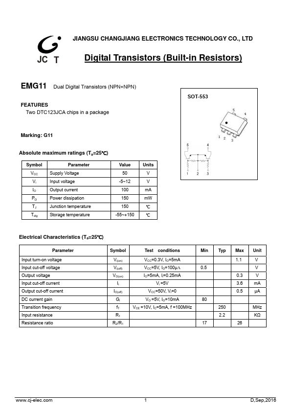
JIANGSU CHANGJIANG ELECTRONICS TECHNOLOGY CO., LTD
JC(T
Digital Transistors (Built-in Resistors)
EMG11 Dual Digital Transistors (NPN+NPN)
FEATURES Two DTC123JCA chips in a package
Marking: G11
Absolute maximum ratings (Ta=25℃)
Symbol VCC Vi IO PD TJ Tstg
Parameter Supply Voltage Input voltage Output current Power dissipation Junction temperature Storage temperature
Value 50
-5~12 100 150 150 -55~+150
Units V V mA
mW
℃ ℃
SOT-553 1
Electrical Characteristics (Ta=25℃)
Parameter
Input turn-on voltage Input cut-off voltage Output voltage Input cut-off current Output cut-off current DC current gain Transition frequency Input resistance Resistance ratio
Symbol
Test conditions
Min Typ Max Unit
Vi(on) Vi(off) VO(on)
Ii IO(off)
Gi fT R1 R2/R1
VCC=0.
 EMG11 Datasheet