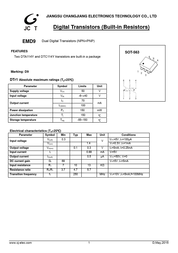
Two DTA114Y and DTC114Y transistors are built-in a package
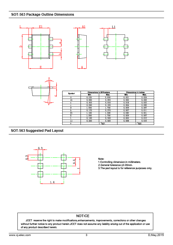
SOT-563
Marking: D9
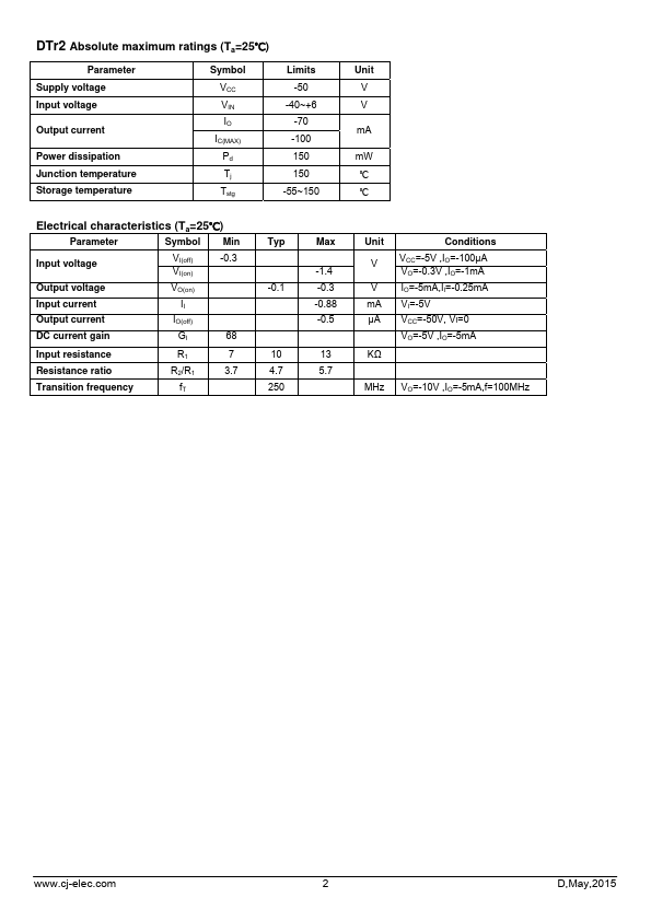
DTr1 Absolute maximum ratings (Ta=25℃)
Parameter Supply voltage Input voltage
Output current
Power dissipation Junction temperature Storage temperature
Symbol VCC VIN IO
IC(MAX) Pd Tj Tstg
Limits 50
-6~+40 70 100
150 150 -55~150
Unit V V
mA
mW ℃ ℃
Electrical characteristics (Ta=25℃)
Parameter
Symbol Min
Input voltage
VI(off) VI(on)
0.3
Output voltage
VO(on)
Input current
II
Output current
IO(off)
D.
The following content is an automatically extracted verbatim text
from the original manufacturer datasheet and is provided for reference purposes only.
View original datasheet text
JC(T
JIANGSU CHANGJIANG ELECTRONICS TECHNOLOGY CO., LTD
Digital Transistors (Built-in Resistors)
EMD9 Dual Digital Transistors (NPN+PNP)
FEATURES Two DTA114Y and DTC114Y transistors are built-in a package
SOT-563
Marking: D9
DTr1 Absolute maximum ratings (Ta=25℃)
Parameter Supply voltage Input voltage
Output current
Power dissipation Junction temperature Storage temperature
Symbol VCC VIN IO
IC(MAX) Pd Tj Tstg
Limits 50
-6~+40 70 100
150 150 -55~150
Unit V V
mA
mW ℃ ℃
Electrical characteristics (Ta=25℃)
Parameter
Symbol Min
Input voltage
VI(off) VI(on)
0.3
Output voltage
VO(on)
Input current
II
Output current
IO(off)
DC current gain
GI 68
Input resistance
R1 7
Resistance ratio
R2/R1
3.7
Transition frequency
fT
Typ
0.1
10 4.7 250
Max
1.4 0.3 0.88 0.5
13 5.
 EMD9 Datasheet