Download the EMD10 datasheet PDF.
This datasheet also covers the EMB10 variant, as both devices belong to the same dual digital transistors family and are provided as variant models within a single manufacturer datasheet.
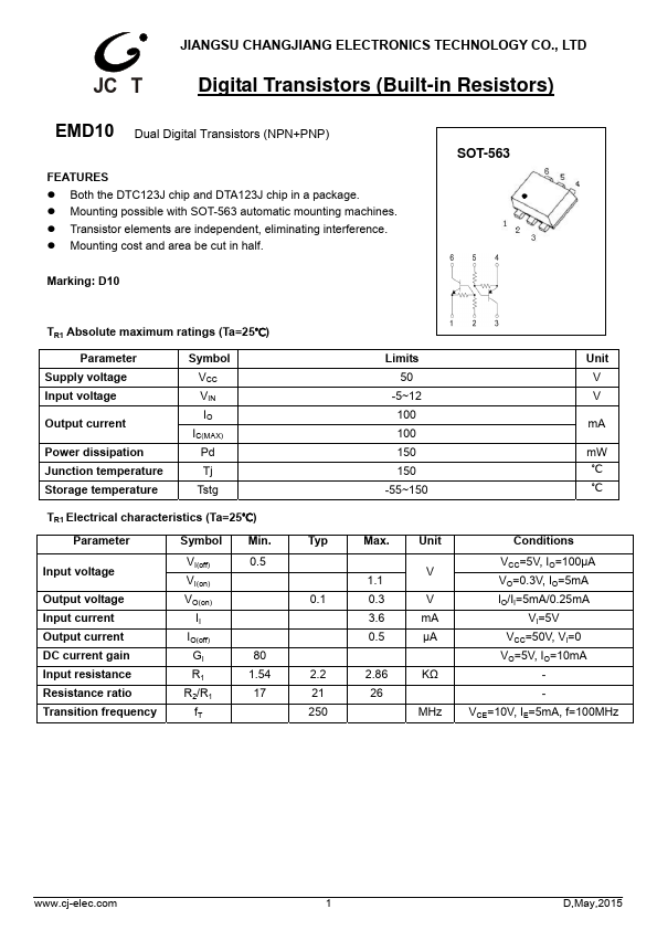
Features
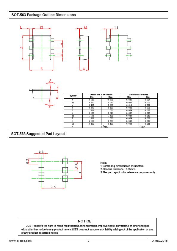
- z Both the DTC123J chip and DTA123J chip in a package. z Mounting possible with SOT-563 automatic mounting machines. z Transistor elements are independent, eliminating interference. z Mounting cost and area be cut in half. SOT-563
Marking: D10
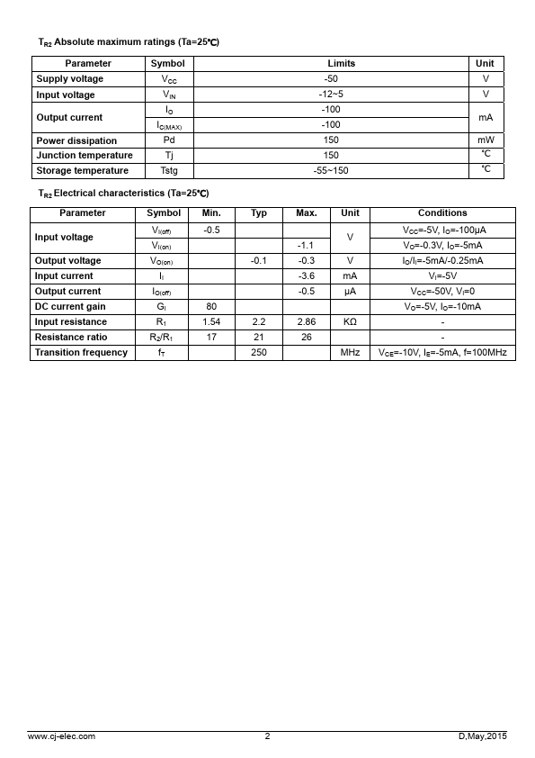
TR1 Absolute maximum ratings (Ta=25℃)
Parameter Supply voltage Input voltage
Output current
Power dissipation Junction temperature Storage temperature
Symbol VCC VIN IO
IC(MAX) Pd Tj Tstg
Limits 50
-5~12 100 100 150 150 -55~150
Unit V V
mA
mW ℃ ℃
T.
 EMD10 Datasheet