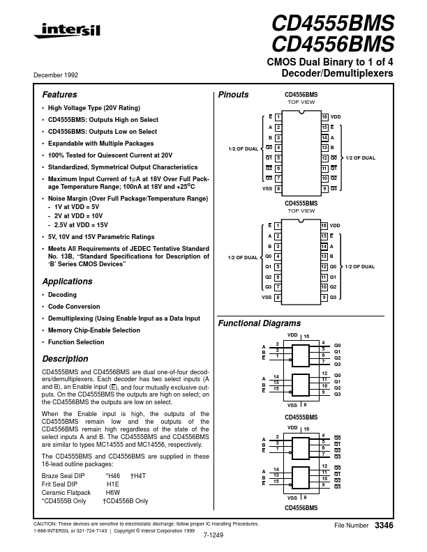
CD4555BMS
Features
- High Voltage Type (20V Rating)
- CD4555BMS: Outputs High on Select
- CD4556BMS: Outputs Low on Select
- Expandable with Multiple Packages
CD4556BMS TOP VIEW
16 VDD 15 E 14 A 13 B 12 Q0 11 Q1 10 Q2 9 Q3 1/2 OF DUAL
1/2 OF DUAL
Q0 Q1 Q2 Q3 VSS
- 100% Tested for Quiescent Current at 20V
- Standardized, Symmetrical Output Characteristics
- Maximum Input Current of 1µA at 18V Over Full Package Temperature Range; 100n A at 18V and +25o C
- Noise Margin (Over Full Package/Temperature Range)
- 1V at VDD = 5V
- 2V at VDD = 10V
- 2.5V at VDD = 15V
- 5V, 10V and 15V Parametric Ratings
- Meets All Requirements of JEDEC Tentative Standard No. 13B, “Standard Specifications for Description of ‘B’ Series CMOS Devices”
1/2 OF DUAL
CD4555BMS TOP VIEW
E A B Q0 Q1 Q2 Q3 VSS 1 2 3 4 5 6 7 8 16 VDD 15 E 14 A 13 B 12 Q0 11 Q1 10 Q2 9 Q3 1/2 OF DUAL
Applications
- Decoding
- Code Conversion
- Demultiplexing (Using Enable Input as a Data Input
- Memory Chip-Enable Selection
- Function...