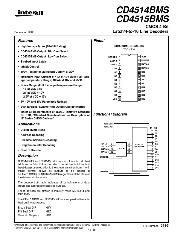
CD4515BMS Key Features
- High-Voltage Types (20-Volt Rating)
- CD4514BMS Output “High” on Select
- CD4515BMS Output “Low” on Select
- Strobed Input Latch
- Inhibit Control
- 100% Tested for Quiescent Current at 20V
- Maximum Input Current of 1µA at 18V Over Full Package Temperature Range; 100nA at 18V and 25oC
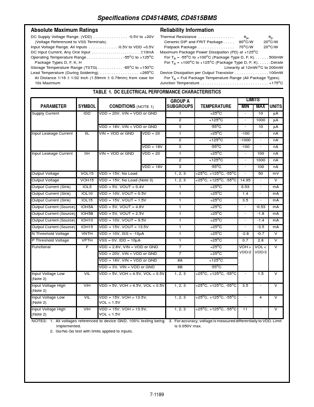
- Noise Margin (Full Package-Temperature Range)
- 1V at VDD = 5V
- 2V at VDD = 10V