CD4512BMS
Description
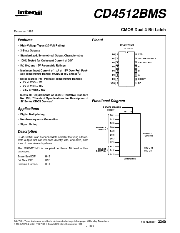
CD4512BMS is an 8-channel data selector featuring a threestate output that can interface directly with, and drive, data lines of bus-oriented systems. The CD4512BMS is supplied in these 16 lead outline packages: Braze Seal DIP Frit Seal DIP Ceramic Flatpack H4S H1E H3X CD4512BMS CAUTION: These devices are sensitive to electrostatic discharge; follow proper IC Handling Procedures. 1-888-INTERSIL or 321-724-7143 | Copyright © Intersil Corporation 1999 File Number 3340 7-1180 Specifications CD4512BMS.
Key Features
- High-Voltage Types (20-Volt Rating)
- 3-State Outputs
- Standardized, Symmetrical Output Characteristics
- 100% Tested for Quiescent Current at 20V
- 5V, 10V, and 15V Parametric Ratings
- Maximum Input Current of 1µA at 18V Over Full Package Temperature Range; 100nA at 18V and 25oC
- Noise Margin (Full Package-Temperature Range): - 1V at VDD = 5V - 2V at VDD = 10V - 2.5V at VDD = 15V
- Meets all Requirements of JEDEC Tentative Standard No. 13B, "Standard Specifications for Description of ‘B’ Series CMOS Devices"