CD4508BMS
Overview
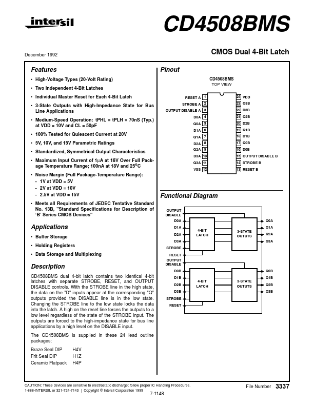
CD4508BMS dual 4-bit latch contains two identical 4-bit latches with separate STROBE, RESET, and OUTPUT DISABLE controls. With the STROBE line in the high state, the data on the "D" inputs appear at the corresponding "Q" outputs provided the DISABLE line is in the low state.
- High-Voltage Types (20-Volt Rating)
- Two Independent 4-Bit Latches
- Individual Master Reset for Each 4-Bit Latch
- 3-State Outputs with High-Impedance State for Bus Line Applications
- Medium-Speed Operation: tPHL = tPLH = 70nS (Typ.) at VDD = 10V and CL = 50pF
- 100% Tested for Quiescent Current at 20V
- 5V, 10V, and 15V Parametric Ratings
- Standardized, Symmetrical Output Characteristics
- Maximum Input Current of 1µA at 18V Over Full Package Temperature Range; 100nA at 18V and 25oC
- Noise Margin (Full Package-Temperature Range): - 1V at VDD = 5V - 2V at VDD = 10V - 2.5V at VDD = 15V