Datasheet Summary
CD4095BMS CD4096BMS
December 1992
CMOS Gated J-K Master-Slave Flip-Flops
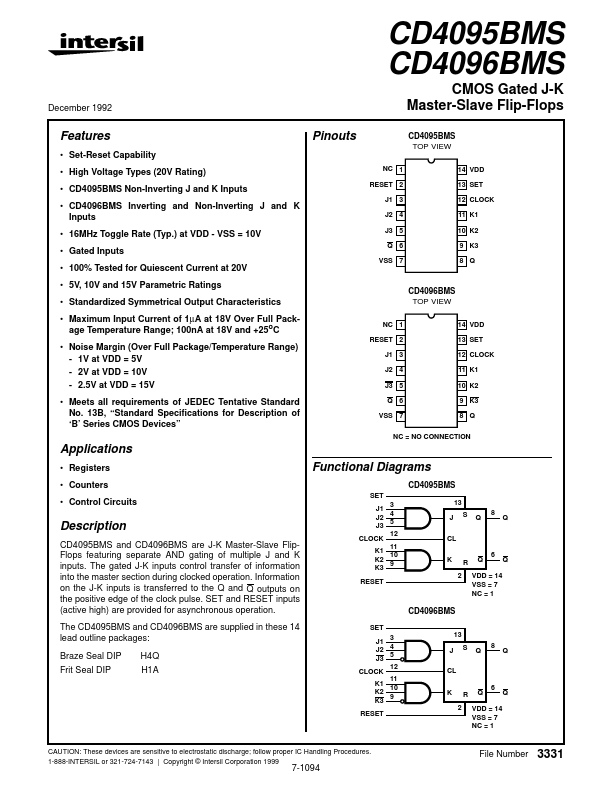
Pinouts
NC 1 RESET 2 J1 3 J2 4 J3 5 Q 6 VSS 7
Features
- Set-Reset Capability
- High Voltage Types (20V Rating)
- CD4095BMS Non-Inverting J and K Inputs
- CD4096BMS Inverting and Non-Inverting J and K Inputs
- 16MHz Toggle Rate (Typ.) at VDD
- VSS = 10V
- Gated Inputs
- 100% Tested for Quiescent Current at 20V
- 5V, 10V and 15V Parametric Ratings
- Standardized Symmetrical Output Characteristics
- Maximum Input Current of 1µA at 18V Over Full Package Temperature Range; 100nA at 18V and +25oC
- Noise Margin (Over Full Package/Temperature Range)
- 1V at VDD = 5V
- 2V at VDD = 10V
- 2.5V at VDD = 15V
- Meets all...