CD4094BMS Overview
Description
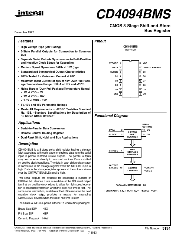
CD4094BMS is a 8-stage serial shift register having a storage latch associated with each stage for strobing data from the serial input to parallel buffered 3-state outputs. The parallel outputs may be connected directly to common bus lines.
Key Features
- High Voltage Type (20V Rating)
- 3-State Parallel Outputs for Connection to Common Bus
- Separate Serial Outputs Synchronous to Both Positive and Negative Clock Edges for Cascading
- Medium Speed Operation
- 5MHz at 10V (typ)