CD4042BMS
CD4042BMS is CMOS Quad Clocked D-Latch manufactured by Intersil.
December 1992
CMOS Quad Clocked “D” Latch
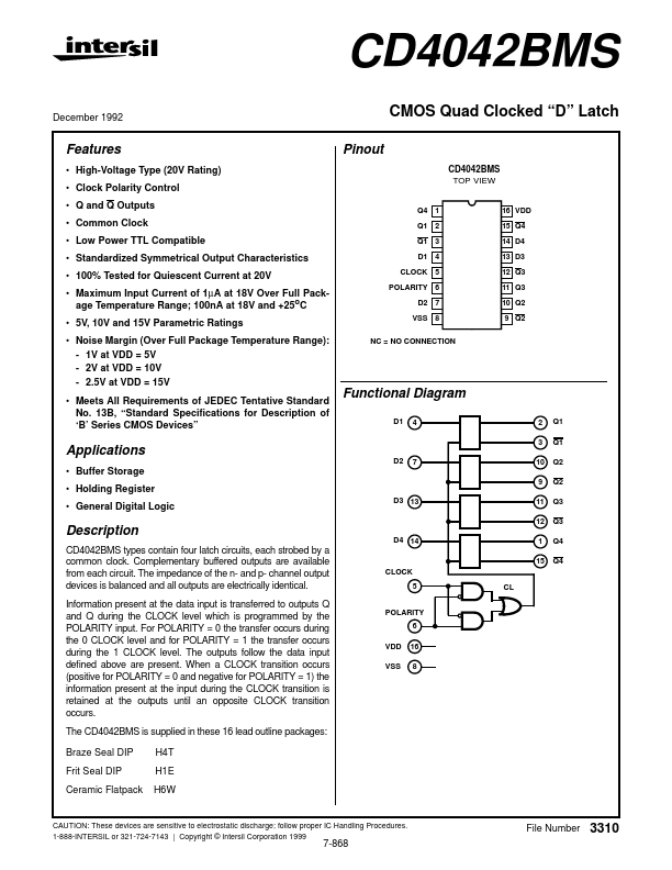
Pinout
CD4042BMS TOP VIEW
Features
- High-Voltage Type (20V Rating)
- Clock Polarity Control
- Q and Q Outputs
- mon Clock
- Low Power TTL patible
- Standardized Symmetrical Output Characteristics
- 100% Tested for Quiescent Current at 20V
- Maximum Input Current of 1µA at 18V Over Full Package Temperature Range; 100n A at 18V and +25o C
- 5V, 10V and 15V Parametric Ratings
- Noise Margin (Over Full Package Temperature Range):
- 1V at VDD = 5V
- 2V at VDD = 10V
- 2.5V at VDD = 15V
- Meets All Requirements of JEDEC Tentative Standard No. 13B, “Standard Specifications for Description of ‘B’ Series CMOS Devices”
Q4 1 Q1 2 Q1 3 D1 4 CLOCK 5 POLARITY 6 D2 7 VSS 8 NC = NO CONNECTION
16 VDD 15 Q4 14 D4 13 D3 12 Q3 11 Q3 10 Q2 9 Q2
Functional Diagram
D1 4 2 3 D2 7 10 9 D3 13 11 12 D4 14 1 15 CLOCK 5 CL Q1 Q1 Q2 Q2 Q3 Q3 Q4 Q4
Applications
- Buffer Storage
- Holding Register
- General Digital Logic
Description
CD4042BMS types contain four latch circuits, each strobed by a mon clock. plementary buffered outputs are available from each circuit. The impedance of the n- and p- channel output devices is balanced and all outputs are electrically identical. Information present at the data input is transferred to outputs Q and Q during the CLOCK level which is programmed by the POLARITY input. For POLARITY = 0 the transfer occurs during the 0 CLOCK level and for POLARITY = 1 the transfer occurs during the 1 CLOCK level. The outputs follow the data input defined above are present. When a CLOCK transition occurs (positive for POLARITY = 0 and negative for POLARITY = 1) the information present at the input during the CLOCK transition is retained at the outputs until an opposite CLOCK transition occurs. The CD4042BMS is supplied in these 16 lead outline packages: Braze Seal DIP Frit Seal DIP Ceramic Flatpack H4T H1E H6W
POLARITY 6 VDD VSS 16...