CD4030BMS
Description
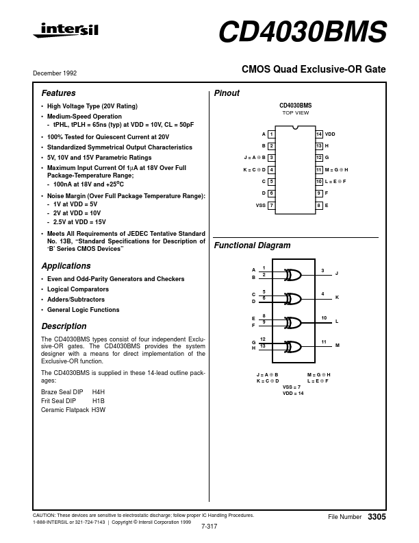
The CD4030BMS types consist of four independent Exclusive-OR gates. The CD4030BMS provides the system designer with a means for direct implementation of the Exclusive-OR function.
Key Features
- High Voltage Type (20V Rating)
- Medium-Speed Operation - tPHL, tPLH = 65ns (typ) at VDD = 10V, CL = 50pF
- 100% Tested for Quiescent Current at 20V
- Standardized Symmetrical Output Characteristics
- 5V, 10V and 15V Parametric Ratings
- Maximum Input Current Of 1µA at 18V Over Full Package-Temperature Range; - 100nA at 18V and +25oC
- Noise Margin (Over Full Package Temperature Range): - 1V at VDD = 5V - 2V at VDD = 10V - 2.5V at VDD = 15V
- Meets All Requirements of JEDEC Tentative Standard No. 13B, “Standard Specifications for Description of ‘B’ Series CMOS Devices”