CD4015BMS Overview
Description
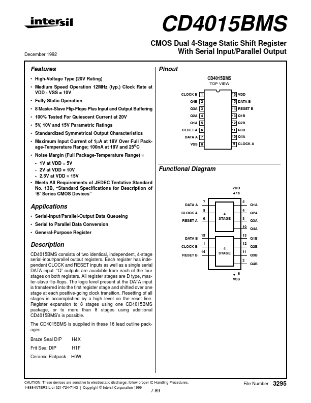
CD4015BMS consists of two identical, independent, 4-stage serial-input/parallel output registers. Each register has independent CLOCK and RESET inputs as well as a single serial DATA input.
Key Features
- High-Voltage Type (20V Rating)
- Medium Speed Operation 12MHz (typ.) Clock Rate at VDD
- Fully Static Operation
- 8 Master-Slave Flip-Flops Plus Input and Output Buffering
- 100% Tested For Quiescent Current at 20V