DATASHEET
CD4011BMS, CD4012BMS, CD4023BMS
CMOS NAND Gates
FN3079
Rev 0.00
November 1994
Features
• High-Voltage Types (20V Rating)
• Propagation Delay Time = 60ns (typ.) at CL = 50pF,
VDD = 10V
• Buffered Inputs and Outputs
• Standardized Symmetrical Output Characteristics
• Maximum Input Current of 1A at 18V Over Full Package-
Temperature Range; 100nA at 18V and +25oC
• 100% Tested for Maximum Quiescent Current at 20V
• 5V, 10V and 15V Parametric Ratings
• Noise Margin (Over Full Package Temperature Range):
- 1V at VDD = 5V
- 2V at VDD = 10V
- 2.5V at VDD = 15V
• Meets All Requirements of JEDEC Tentative Standards
No. 13B, “Standard Specifications for Description of
“B” Series CMOS Device’s
Description
CD4011BMS - Quad 2 Input
CD4012BMS - Dual 4 Input
CD4023BMS - Triple 3 Input
CD4011BMS, CD4012BMS, and CD4023BMS NAND gates
provide the system designer with direct implementation of
the NAND function and supplement the existing family of
CMOS gates. All inputs and outputs are buffered.
The CD4011BMS, CD4012BMS and the CD4023BMS is
supplied in these 14 lead outline packages:
Braze Seal DIP
Frit Seal DIP
Ceramic Flatpack
CD4011B
H4Q
H1B
H3W
CD4012B
H4H
H1B
H3W
CD4023B
H4Q
H1B
H3W
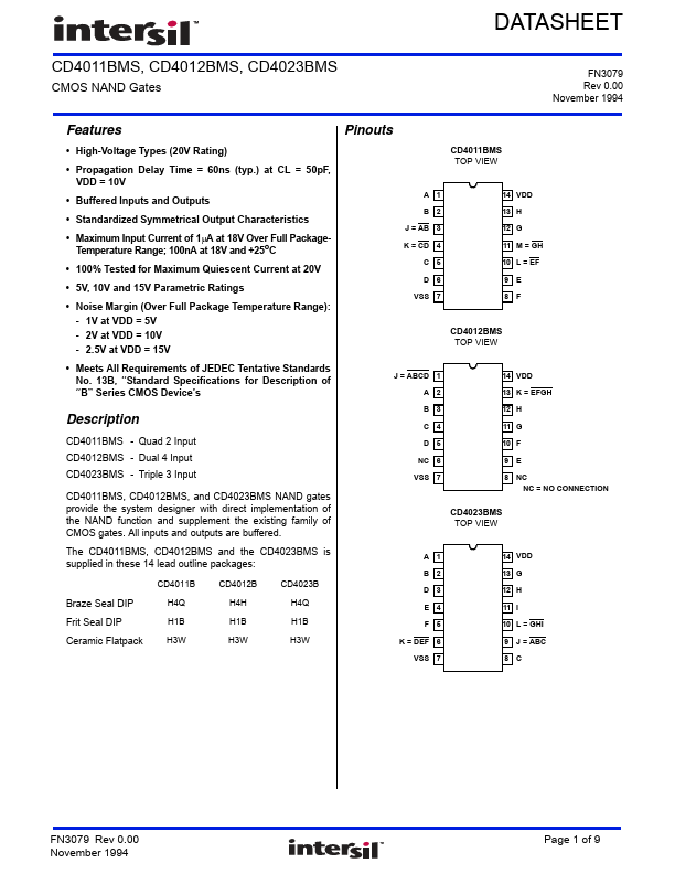
Pinouts
CD4011BMS
TOP VIEW
A1
B2
J = AB 3
K = CD 4
C5
D6
VSS 7
14 VDD
13 H
12 G
11 M = GH
10 L = EF
9E
8F
CD4012BMS
TOP VIEW
J = ABCD 1
A2
B3
C4
D5
NC 6
VSS 7
14 VDD
13 K = EFGH
12 H
11 G
10 F
9E
8 NC
NC = NO CONNECTION
CD4023BMS
TOP VIEW
A1
B2
D3
E4
F5
K = DEF 6
VSS 7
14 VDD
13 G
12 H
11 I
10 L = GHI
9 J = ABC
8C
FN3079 Rev 0.00
November 1994
Page 1 of 9