CD40109BMS
Description
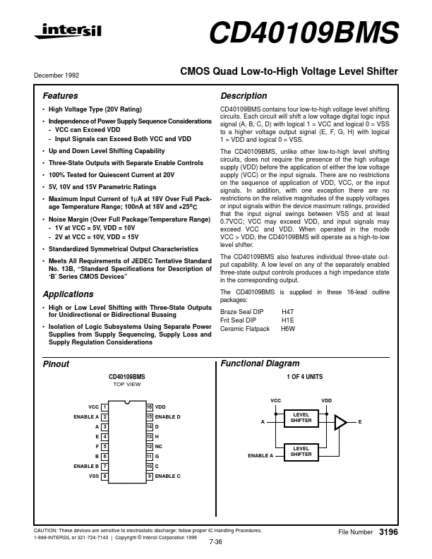
CD40109BMS contains four low-to-high voltage level shifting circuits. Each circuit will shift a low voltage digital logic input signal (A, B, C, D) with logical 1 = VCC and logical 0 = VSS to a higher voltage output signal (E, F, G, H) with logical 1 = VDD and logical 0 = VSS.
Key Features
- High Voltage Type (20V Rating)
- Independence of Power Supply Sequence Considerations - VCC can Exceed VDD - Input Signals can Exceed Both VCC and VDD
- Up and Down Level Shifting Capability
- Three-State Outputs with Separate Enable Controls
- 100% Tested for Quiescent Current at 20V
- 5V, 10V and 15V Parametric Ratings
- Maximum Input Current of 1µA at 18V Over Full Package Temperature Range; 100nA at 18V and +25oC
- Noise Margin (Over Full Package/Temperature Range) - 1V at VCC = 5V, VDD = 10V - 2V at VCC = 10V, VDD = 15V
- Standardized Symmetrical Output Characteristics
- Meets All Requirements of JEDEC Tentative Standard No. 13B, “Standard Specifications for Description of ‘B’ Series CMOS Devices”