Datasheet4U Logo Datasheet4U.com

CD4007UBMS - CMOS Dual Complementary Pair Plus Inverter

Description

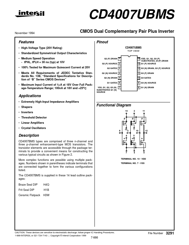
of “B” Series CMOS Devices” Maximum Input Current of 1µA at 18V Over Full Package-Temperature Range; 100nA at 18V and +25oC 14 VDD, Q1, Q2, Q3 (P) SUBSTRATES, Q1(P) DRAIN 13 Q1 (P) SOURCE 12 Q3 (N) DRAIN, Q3 (P) SOURCE 11 Q3 (P) DRAIN 10 Q3 GATES 9 Q3 (N) SOURCE 8 Q1 (N) DRAIN 7 Applic

Features

  • High-Voltage Type (20V Rating).
  • Standardized Symmetrical Output Characteristics.
  • Medium Speed Operation - tPHL, tPLH = 30 ns (typ) at 10V.
  • 100% Tested for Maximum Quiescent Current at 20V.
  • Meets All Requirements of JEDEC Tentative Standards No. 13B, “Standard Specifications for.

📥 Download Datasheet

Datasheet preview – CD4007UBMS

Datasheet Details

Part number CD4007UBMS
Manufacturer Intersil
File Size 104.82 KB
Description CMOS Dual Complementary Pair Plus Inverter
Datasheet download datasheet CD4007UBMS Datasheet
Additional preview pages of the CD4007UBMS datasheet.
Other Datasheets by Intersil Corporation

Full PDF Text Transcription

Click to expand full text
CD4007UBMS November 1994 CMOS Dual Complementary Pair Plus Inverter Pinout CD4007UBMS TOP VIEW Q2 (P) DRAIN 1 Q2 (P) SOURCE 2 Q2 GATES 3 Q2 (N) SOURCE 4 Q2 (N) DRAIN 5 Q1 GATES 6 VSS, Q1, Q2, Q3 (N) SUBSTRATES Q1 (N) SOURCE Features • High-Voltage Type (20V Rating) • Standardized Symmetrical Output Characteristics • Medium Speed Operation - tPHL, tPLH = 30 ns (typ) at 10V • 100% Tested for Maximum Quiescent Current at 20V • Meets All Requirements of JEDEC Tentative Standards No.
Published: |