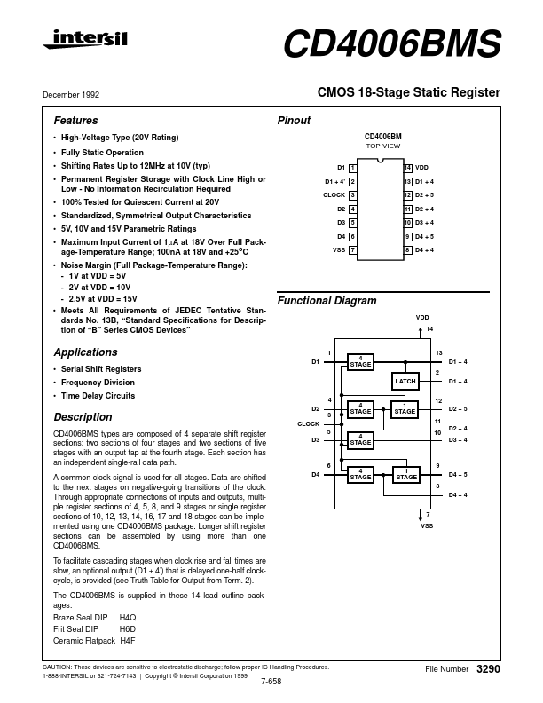
Datasheet4U Logo Datasheet4U.com

CD4006BMS - CMOS 18-Stage Static Register

Datasheet Summary

Description

of “B” Series CMOS Devices” CD4006BM TOP VIEW D1 1 D1 + 4’ 2 CLOCK 3 D2 4 D3 5 D4 6 VSS 7 14 VDD 13 D1 + 4 12 D2 + 5 11 D2 + 4 10 D3 + 4 9 D4 + 5 8 D4 + 4 Functional Diagram VDD 14 Applications Serial Shift Registers Frequency Division Tim

Features

  • Pinout.
  • High-Voltage Type (20V Rating).
  • Fully Static Operation.
  • Shifting Rates Up to 12MHz at 10V (typ).
  • Permanent Register Storage with Clock Line High or Low - No Information Recirculation Required.
  • 100% Tested for Quiescent Current at 20V.
  • Standardized, Symmetrical Output Characteristics.
  • 5V, 10V and 15V Parametric Ratings.
  • Maximum Input Current of 1µA at 18V Over Full Pack- age-Temperature Range; 100nA at 18V and +25oC.

📥 Download Datasheet

Datasheet preview – CD4006BMS

Datasheet Details

Part number CD4006BMS
Manufacturer Intersil Corporation
File Size 76.00 KB
Description CMOS 18-Stage Static Register
Datasheet download datasheet CD4006BMS Datasheet
Additional preview pages of the CD4006BMS datasheet.
Other Datasheets by Intersil Corporation

Full PDF Text Transcription

Click to expand full text
CD4006BMS December 1992 CMOS 18-Stage Static Register Features Pinout • High-Voltage Type (20V Rating) • Fully Static Operation • Shifting Rates Up to 12MHz at 10V (typ) • Permanent Register Storage with Clock Line High or Low - No Information Recirculation Required • 100% Tested for Quiescent Current at 20V • Standardized, Symmetrical Output Characteristics • 5V, 10V and 15V Parametric Ratings • Maximum Input Current of 1µA at 18V Over Full Pack- age-Temperature Range; 100nA at 18V and +25oC • Noise Margin (Full Package-Temperature Range): - 1V at VDD = 5V - 2V at VDD = 10V - 2.5V at VDD = 15V • Meets All Requirements of JEDEC Tentative Standards No.
Published: |