CD22M3493
CD22M3493 is 12 x 8 x 1 BiMOS-E Crosspoint Switch manufactured by Intersil.
Data Sheet January 1997 File Number
12 x 8 x 1 Bi MOS-E Crosspoint Switch
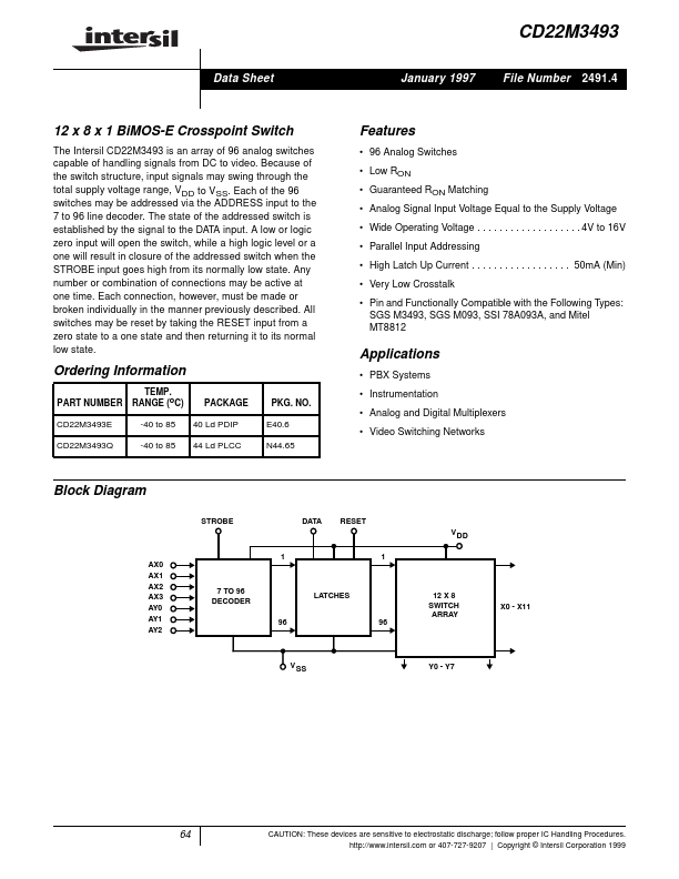
The Intersil CD22M3493 is an array of 96 analog switches capable of handling signals from DC to video. Because of the switch structure, input signals may swing through the total supply voltage range, VDD to VSS. Each of the 96 switches may be addressed via the ADDRESS input to the 7 to 96 line decoder. The state of the addressed switch is established by the signal to the DATA input. A low or logic zero input will open the switch, while a high logic level or a one will result in closure of the addressed switch when the STROBE input goes high from its normally low state. Any number or bination of connections may be active at one time. Each connection, however, must be made or broken individually in the manner previously described. All switches may be reset by taking the RESET input from a zero state to a one state and then returning it to its normal low state.
Features
- 96 Analog Switches
- Low RON
- Guaranteed RON Matching
- Analog Signal Input Voltage Equal to the Supply Voltage
- Wide Operating Voltage
- -
- . . . . 4V to 16V
- Parallel Input Addressing
- High Latch Up Current
- -
- . . . 50m A (Min)
- Very Low Crosstalk
- Pin and Functionally patible with the Following Types: SGS M3493, SGS M093, SSI 78A093A, and Mitel MT8812
[ /Title () /Subject () /Autho r () /Keywords () /Creator () /DOCI NFO pdfmark
Applications
- PBX Systems
- Instrumentation
Ordering Information
PART NUMBER CD22M3493E CD22M3493Q TEMP. RANGE (o C) -40 to 85 -40 to 85 PACKAGE 40 Ld PDIP 44 Ld PLCC PKG. NO.
[ /Page Mode /Use Outlines /DOCVIEW pdfmark
- Analog and Digital Multiplexers
E40.6 N44.65
- Video Switching Networks
Block Diagram
STROBE DATA RESET V DD 1 AX0 AX1 AX2 AX3 AY0 AY1 AY2 1
7 TO 96 DECODER...